SLVSEJ1A
February 2021 – May 2022
TLC6983
PRODUCTION DATA
1
Features
2
Applications
3
Description
4
Revision History
5
Description (continued)
6
Pin Configuration and Functions
7
Specifications
7.1
Absolute Maximum Ratings
7.2
ESD Ratings
7.3
Recommended Operating Conditions
7.4
Thermal Information
7.5
Electrical Characteristics
7.6
Timing Requirements
7.7
Switching Characteristics
7.8
Typical Characteristics
8
Detailed Description
8.1
Overview
8.2
Functional Block Diagram
8.3
Feature Description
8.3.1
Independent and Stackable Mode
8.3.1.1
Independent Mode
8.3.1.2
Stackable Mode
8.3.2
Current Setting
8.3.2.1
Brightness Control (BC) Function
8.3.2.2
Color Brightness Control (CC) Function
8.3.2.3
Choosing BC and CC for a Different Application
8.3.3
Frequency Multiplier
8.3.4
Line Transitioning Sequence
8.3.5
Protections and Diagnostics
8.3.5.1
Thermal Shutdown Protection
8.3.5.2
IREF Resistor Short Protection
8.3.5.3
LED Open Load Detection and Removal
8.3.5.3.1
LED Open Detection
8.3.5.3.2
Read LED Open Information
8.3.5.3.3
LED Open Caterpillar Removal
8.3.5.4
LED Short/Weak Short Circuitry Detection and Removal
8.3.5.4.1
LED Short/Weak Short Detection
8.3.5.4.2
Read LED Short Information
8.3.5.4.3
LSD Caterpillar Removal
8.4
Device Functional Modes
8.5
Continuous Clock Series Interface
8.5.1
Data Validity
8.5.2
CCSI Frame Format
8.5.3
Write Command
8.5.3.1
Chip Index Write Command
8.5.3.2
VSYNC Write Command
8.5.3.3
Soft_Reset Command
8.5.3.4
Data Write Command
8.5.4
Read Command
8.6
PWM Grayscale Control
8.6.1
Grayscale Data Storage and Display
8.6.1.1
Memory Structure Overview
8.6.1.2
Details of Memory Bank
8.6.1.3
Write a Frame Data into Memory Bank
8.6.2
PWM Control for Display
8.7
Register Maps
8.7.1
FC0
8.7.2
FC1
8.7.3
FC2
8.7.4
FC3
8.7.5
FC4
8.7.6
FC10
8.7.7
FC11
8.7.8
FC12
8.7.9
FC13
8.7.10
FC14
8.7.11
FC15
9
Application and Implementation
9.1
Application Information
9.2
Typical Application
9.2.1
Design Requirements
9.2.1.1
System Structure
9.2.1.2
SCLK Frequency
9.2.1.3
Internal GCLK Frequency
9.2.1.4
Line Switch Time
9.2.1.5
Blank Time Removal
9.2.1.6
BC and CC
9.2.2
Detailed Design Procedure
9.2.2.1
Chip Index Command
9.2.2.2
FC Registers Settings
9.2.2.3
Grayscale Data Write
9.2.2.4
VSYNC Command
9.2.2.5
LED Open and Short Read
9.2.3
Application Curves
10
Power Supply Recommendations
11
Layout
11.1
Layout Guidelines
11.2
Layout Example
12
Device and Documentation Support
12.1
Documentation Support
12.1.1
Related Documentation
12.2
Receiving Notification of Documentation Updates
12.3
Support Resources
12.4
Trademarks
12.5
Electrostatic Discharge Caution
12.6
Glossary
13
Mechanical, Packaging, and Orderable Information
Package Options
Mechanical Data (Package|Pins)
RRF|76
MPQF556
ZXL|96
MPBGAU1
Thermal pad, mechanical data (Package|Pins)
Orderable Information
slvsej1a_oa
slvsej1a_pm
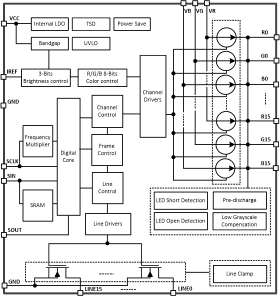
8.2
Functional Block Diagram