-
TLC6C5716-Q1 Automotive 16-Channel, Full Diagnostics, Constant-Current LED Driver
- 1 Features
- 2 Applications
- 3 Description
- 4 Revision History
- 5 Pin Configuration and Functions
- 6 Specifications
-
7 Detailed Description
- 7.1 Overview
- 7.2 Functional Block Diagram
- 7.3
Feature Description
- 7.3.1 Maximum Constant-Sink-Current Setting
- 7.3.2 Brightness Control and Dot Correction
- 7.3.3 Grayscale Configuration
- 7.3.4
Diagnostics
- 7.3.4.1 LED Diagnostics
- 7.3.4.2 Adjacent-Pin-Short Check
- 7.3.4.3 IREF-Short and IREF-Open Detection
- 7.3.4.4 Pre-Thermal Warning Flag
- 7.3.4.5 Thermal Error Flag
- 7.3.4.6 Negate-Bit Toggle
- 7.3.4.7 LOD_LSD Self-Test
- 7.3.4.8 ERR Pin
- 7.3.4.9 ERROR Clear
- 7.3.4.10 Global Reset
- 7.3.4.11 Slew Rate Control
- 7.3.4.12 Channel Group Delay
- 7.4 Device Functional Modes
- 7.5 Programming
- 7.6 Register Maps
- 8 Application and Implementation
- 9 Power Supply Recommendations
- 10Layout
- 11Device and Documentation Support
- 12Mechanical, Packaging, and Orderable Information
- IMPORTANT NOTICE
Package Options
Mechanical Data (Package|Pins)
- DAP|38
Thermal pad, mechanical data (Package|Pins)
TLC6C5716-Q1 Automotive 16-Channel, Full Diagnostics, Constant-Current LED Driver
1 Features
- AEC-Q100 Qualified for Automotive Applications
- Device Temperature Grade 1: –40°C to 125°C, TA
- 16 Constant-Current-Sink Output Channels
- 50-mA Maximum Output Current
- 8-V Maximum Output Voltage
- Two Output Groups: OUTRn, OUTBn
- Output Current Adjustment
- 7-Bit Dot Correction (DC) for Each Channel
- 8-Bit Brightness Control (BC) for Each Group
- Integrated PWM Grayscale Generator
- PWM Dimming for Each Individual Channel
- Adjustable Global Grayscale Mode: 12-Bit, 10-Bit, 8-Bit
- Protection and Diagnostics
- LED-Open Detection (LOD), LED-Short Detection (LSD), Output Short-to-GND Detection (OSD)
- Adjacent-Pin Short (APS) Detection
- Pre-Thermal Warning (PTW), Thermal Shutdown (TSD)
- IREF Resistor Open- (IOF) and Short-Detection (ISF) and -Protection
- Negate Bit Toggle for GCLK Error Detect and LOD_LSD Register Error Check
- LOD_LSD Circuit Self-Test
- Programmable Output Slew Rate
- Output Channel Group Delay
- Serial Data Interface
2 Applications
- Automotive Cluster
- Automotive Local Dimming Display
- Automotive Faceplate
- Automotive HVAC Control Panel
- Automotive Center Stack Display
- Automotive Interior and RGB Ambient Lighting
- Automotive Shift-by-Wire and Gear Shifter
3 Description
There are automotive applications for indicators and for LCD local-dimming backlighting. For these applications, more persons think multi-channel constant-current LED drivers are necessary. The requirement is to get the same intensity and color temperature of LEDs. For system-level safety, it is necessary that the LED drivers can sense faults.
The TLC6C5716-Q1 device is an automotive 16-channel constant-current RGB LED driver that can do tests on the LEDs. The TLC6C5716-Q1 device supplies a maximum of 50-mA output current set by an external resistor. The device has a 7-bit dot correction with two ranges for each output. The device also has an 8-bit intensity control for the outputs of each color group.
A 12-,10-, or 8-bit grayscale control adjusts the intensity of each output. The device has circuits that sense faults in the system, including LED faults, adjacent-pin short faults, reference-resistor faults, and more. A slew rate control has 2 positions for adjustment to get the largest decrease in system noise. There is an interval between the changes of output level from one LED group to a different one. This interval helps to decrease the starting electrical current. The SDI and SDO pins let more than one device be connected in series for control through 1 serial interface.
Device Information(1)
| PART NUMBER | PACKAGE | BODY SIZE (NOM) |
|---|---|---|
| TLC6C5716-Q1 | HTSSOP (38) | 6.20 mm × 12.50 mm |
- For all available packages, see the orderable addendum at the end of the data sheet.
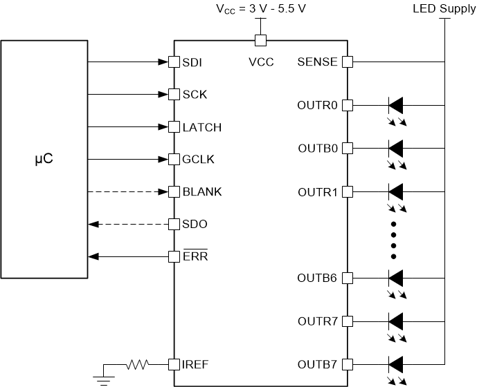
Typical Application Schematic

4 Revision History
Changes from * Revision (July 2018) to A Revision
- Changed the description for GCLK in Go
- Changed "indicates" to "initiates" in the Global Reset sectionGo
- Added "the SID" to the Fault Mode section to identify the register where the overtemperature fault is latchedGo
- Changed "APS time" to "APS detection time" for bit 199 in Table 12Go
- Changed "24 zones" to "16 zones" and "six TLC6C5716-Q1 units" to "eight TLC6C5716-Q1 units" in the Detailed Design Procedure section Go
- Added a new sentence preceding Figure 32Go
- Added the Application Curves sectionGo
- Added two sentences to the Power Supply Recommendations sectionGo