SLASEK2A December 2017 – August 2018 TLC6C5724-Q1
PRODUCTION DATA.
- 1 Features
- 2 Applications
- 3 Description
- 4 Revision History
- 5 Pin Configuration and Functions
- 6 Specifications
-
7 Detailed Description
- 7.1 Overview
- 7.2 Functional Block Diagram
- 7.3
Feature Description
- 7.3.1 Maximum Constant-Sink-Current Setting
- 7.3.2 Brightness Control and Dot Correction
- 7.3.3 Grayscale Configuration
- 7.3.4
Diagnostics
- 7.3.4.1 LED Diagnostics
- 7.3.4.2 Adjacent-Pin-Short Check
- 7.3.4.3 IREF Short and IREF Open Detection
- 7.3.4.4 Pre-Thermal Warning Flag
- 7.3.4.5 Thermal Error Flag
- 7.3.4.6 Negate Bit Toggle
- 7.3.4.7 LOD_LSD Self-Test
- 7.3.4.8 ERR Pin
- 7.3.4.9 ERROR Clear
- 7.3.4.10 Global Reset
- 7.3.4.11 Slew Rate Control
- 7.3.4.12 Channel Group Delay
- 7.4 Device Functional Modes
- 7.5 Programming
- 7.6 Register Maps
- 8 Application and Implementation
- 9 Power Supply Recommendations
- 10Layout
- 11Device and Documentation Support
- 12Mechanical, Packaging, and Orderable Information
Package Options
Mechanical Data (Package|Pins)
- DAP|38
Thermal pad, mechanical data (Package|Pins)
3 Description
There are automotive applications for indicators and for LCD local-dimming backlighting. For these applications, more persons think multi-channel constant-current LED drivers are necessary. The requirement is to get the same intensity and color temperature of LEDs. For system-level safety, it is necessary that the LED drivers can sense faults.
The TLC6C5724-Q1 device is an automotive 24-channel constant-current RGB LED driver that can do tests on the LEDs. The TLC6C5724-Q1 device supplies a maximum of 50‑mA output current set by an external resistor. The device has a 7-bit dot correction with two ranges for each output. The device also has an 8-bit intensity control for the outputs of each color group. A 12-,10-, or 8-bit grayscale control adjusts the intensity of each output. The device has circuits that sense faults in the system, including LED faults, adjacent-pin short faults, reference-resistor faults, and more. A slew rate control has 2 positions for adjustment to get the largest decrease in system noise. There is an interval between the changes of output level from one LED group to a different one. This interval helps to decrease the starting electrical current. The SDI and SDO pins let more than one device be connected in series for control through one serial interface.
Device Information(1)
| PART NUMBER | PACKAGE | BODY SIZE (NOM) |
|---|---|---|
| TLC6C5724-Q1 | HTSSOP (38) | 6.20 mm × 12.50 mm |
- For all available packages, see the orderable addendum at the end of the data sheet.
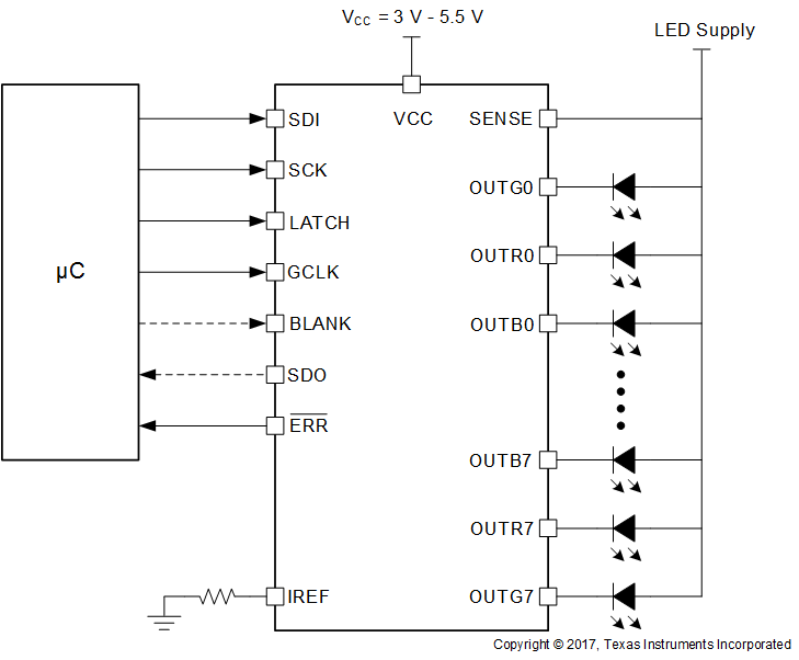
Typical Application Schematic
