SLASEK2A December 2017 – August 2018 TLC6C5724-Q1
PRODUCTION DATA.
- 1 Features
- 2 Applications
- 3 Description
- 4 Revision History
- 5 Pin Configuration and Functions
- 6 Specifications
-
7 Detailed Description
- 7.1 Overview
- 7.2 Functional Block Diagram
- 7.3
Feature Description
- 7.3.1 Maximum Constant-Sink-Current Setting
- 7.3.2 Brightness Control and Dot Correction
- 7.3.3 Grayscale Configuration
- 7.3.4
Diagnostics
- 7.3.4.1 LED Diagnostics
- 7.3.4.2 Adjacent-Pin-Short Check
- 7.3.4.3 IREF Short and IREF Open Detection
- 7.3.4.4 Pre-Thermal Warning Flag
- 7.3.4.5 Thermal Error Flag
- 7.3.4.6 Negate Bit Toggle
- 7.3.4.7 LOD_LSD Self-Test
- 7.3.4.8 ERR Pin
- 7.3.4.9 ERROR Clear
- 7.3.4.10 Global Reset
- 7.3.4.11 Slew Rate Control
- 7.3.4.12 Channel Group Delay
- 7.4 Device Functional Modes
- 7.5 Programming
- 7.6 Register Maps
- 8 Application and Implementation
- 9 Power Supply Recommendations
- 10Layout
- 11Device and Documentation Support
- 12Mechanical, Packaging, and Orderable Information
Package Options
Mechanical Data (Package|Pins)
- DAP|38
Thermal pad, mechanical data (Package|Pins)
6.5 Electrical Characteristics
VCC = 3 V to 5.5 V,TJ=–40°Cto150°C,VSENSE = 5 V, GS = FFFh, BC = FFh, DC= 7Fh with upperDCrange(unlessotherwise noted)| PARAMETER | TEST CONDITIONS | MIN | TYP | MAX | UNIT | |
|---|---|---|---|---|---|---|
| POWER SUPPLIES | ||||||
| ICC | Supply current | SDI, SCK, LATCH = L, BLANK = L, GCLK = L, VOUT = 1 V, IOUT = 2 mA | 4.2 | 5.5 | mA | |
| SDI, SCK, LATCH = L, BLANK = L, GCLK = L, VOUT = 1 V, IOUT = 20 mA | 7.7 | 9 | ||||
| SDI, SCK, LATCH = L, BLANK = H, GCLK = 8 MHz, VOUT = 1 V, IOUT = 20 mA , auto-repeat on | 8.3 | 10 | ||||
| SDI, SCK, LATCH = L, BLANK = H, GCLK = 8 MHz, VOUT = 1 V, IOUT = 50 mA , auto-repeat on | 13.5 | 16 | ||||
| LOGIC INPUTS (SDI, SCK, LATCH, GCLK, BLANK) | ||||||
| IIkg | Input leakage current | At SDI, SCK, LATCH, with VI = VCC; or at SDI, SCK, LATCH, BLANK, GCLK, with VI = GND | –1 | 1 | µA | |
| Rpd | Pull down resistance at BLANK, GCLK | 250 | 500 | 750 | kΩ | |
| CONTROL OUTPUTS (IREF, ERR, SDO) | ||||||
| VIREF | IREF voltage | RIREF = 0.96 kΩ | 1.17 | 1.2 | 1.23 | V |
| VOH | High-level output voltage | At SDO, IOH = –1 mA | VCC – 0.4 | VCC | V | |
| VOL | Low-level output voltage | At SDO, IOL = 1 mA | 0.4 | V | ||
| VERR | ERR pin open-drain voltage drop | IERR = 4 mA | 0.1 VCC | V | ||
| ILKG_ERR | ERR pin leakage current | VERR = 5 V | 1 | µA | ||
| OUTPUT STAGE | ||||||
| V(OUT,min) | Minimum output voltage | VCC = 3.6 V, IOUT = 50 mA | 0.67 | V | ||
| VCC = 3 V, IOUT = 50 mA | 0.7 | |||||
| K(OUT) | Ratio of output current to IREF current, K = I(OUTx) / I(IREF) | 40 | mA/mA | |||
| Ilkg(OUT) | Output leakage current | BLANK = L, VOUT = 7 V, VSENSE = 7 V | 0.1 | µA | ||
| CHANNEL ACCURACY | ||||||
| I(OUT) | Constant output current | VOUT = 1 V, RIREF = 24 kΩ | 1.86 | 2 | 2.14 | mA |
| VOUT = 1 V, RIREF = 0.96 kΩ | 46.5 | 50 | 53.5 | |||
| VOUT = 1V, RIREF open or short | 7 | 10 | 13 | |||
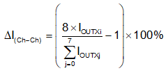
| ΔI(Ch-Ch)(1) | Current accuracy (channel-to-channel in same color group) | VOUT = 1 V, IOUT = 50 mA | –4% | 4% | ||
| VOUT = 1 V, IOUT = 2 mA | –4% | 4% | ||||
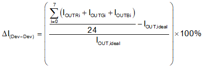
| ΔI(Dev-Dev)(2) | Current accuracy (device-to-device) | VOUT= 1 V, IOUT = 50 mA | –4% | 4% | ||
| VOUT = 1 V, IOUT = 2 mA | -–4% | 4% | ||||
| ΔI(Ch-Ideal)(3) | Current accuracy (channel-to-ideal output) | VOUT = 1 V, IOUT = 50 mA | –7% | 7% | ||
| VOUT = 1 V, IOUT = 2 mA | –7% | 7% | ||||
| ΔI(OUT-VCC)(4) | Line regulation | VOUT = 1 V, VCC = 3 V to 5.5 V, IOUT = 50 mA | –0.7 | 0.7 | %/V | |
| VOUT = 1 V, VCC = 3 V to 5.5 V, IOUT = 2 mA | –0.7 | 0.7 | ||||
| ΔI(OUT-VOUT(5) | Load regulation | VOUT = 1 V to 3 V, IOUT = 50 mA | –0.7 | 0.7 | %/V | |
| VOUT = 1 V to 3 V, IOUT = 2 mA | –0.7 | 0.7 | ||||
| PROTECTION CIRCUITS | ||||||
| VLOD1 | LED open-circuit detection low threshold | LOD_VOLTAGE = 0b | 0.275 | 0.3 | 0.32 | V |
| VLOD2 | LED open-circuit detection high threshold | LOD_VOLTAGE = 1b | 0.48 | 0.5 | 0.52 | V |
| VLSD1 | LED short-circuit detection high threshold | LSD_VOLTAGE = 0b | VSENSE – 0.4 | VSENSE – 0.3 | VSENSE – 0.2 | V |
| VLSD2 | LED short-circuit detection low threshold | LSD_VOLTAGE= 1b | VSENSE – 0.8 | VSENSE – 0.7 | VSENSE – 0.6 | V |
| IIREF_OC | IREF resistor open-circuit detection threshold | VCC = 5 V | 8 | 10 | 12 | µA |
| IIREF_OCHYS | IREF resistor open-circuit detection threshold hysteresis | VCC = 5 V | 5 | µA | ||
| IIREF_SC | IREF resistor short-circuit-detection threshold | VCC = 5 V | 2 | 2.7 | 3.2 | mA |
| IIREF_SCHYS | IREF resistor short-circuit-detection threshold hysteresis | VCC = 5 V | 0.3 | mA | ||
| TPTW | Pre-thermal warning flag threshold | Junction temperature | 125 | 135 | 145 | °C |
| THYS_PTW | Pre-thermal warning flag hysteresis | Junction temperature | 10 | °C | ||
| TSD | Thermal error flag threshold | Junction temperature | 150 | 160 | 170 | °C |
| THYS_TEF | Thermal error flag hysteresis | Junction temperature | 10 | °C | ||
(1) Channel to channel accuracy in thesamecolorgroupiscalculated by the formula below. (X = color group; i,j = 0 to 7 )


(2) Device to device accuracy iscalculatedbytheformulabelow.


(3) Channel to ideal accuracy is calculated bytheformulabelow.


(4) Line regulation accuracy iscalculatedbytheformulabelow.


(5) Load regulation accuracy iscalculatedbytheformulabelow.

