SLASEK2A December 2017 – August 2018 TLC6C5724-Q1
PRODUCTION DATA.
- 1 Features
- 2 Applications
- 3 Description
- 4 Revision History
- 5 Pin Configuration and Functions
- 6 Specifications
-
7 Detailed Description
- 7.1 Overview
- 7.2 Functional Block Diagram
- 7.3
Feature Description
- 7.3.1 Maximum Constant-Sink-Current Setting
- 7.3.2 Brightness Control and Dot Correction
- 7.3.3 Grayscale Configuration
- 7.3.4
Diagnostics
- 7.3.4.1 LED Diagnostics
- 7.3.4.2 Adjacent-Pin-Short Check
- 7.3.4.3 IREF Short and IREF Open Detection
- 7.3.4.4 Pre-Thermal Warning Flag
- 7.3.4.5 Thermal Error Flag
- 7.3.4.6 Negate Bit Toggle
- 7.3.4.7 LOD_LSD Self-Test
- 7.3.4.8 ERR Pin
- 7.3.4.9 ERROR Clear
- 7.3.4.10 Global Reset
- 7.3.4.11 Slew Rate Control
- 7.3.4.12 Channel Group Delay
- 7.4 Device Functional Modes
- 7.5 Programming
- 7.6 Register Maps
- 8 Application and Implementation
- 9 Power Supply Recommendations
- 10Layout
- 11Device and Documentation Support
- 12Mechanical, Packaging, and Orderable Information
Package Options
Mechanical Data (Package|Pins)
- DAP|38
Thermal pad, mechanical data (Package|Pins)
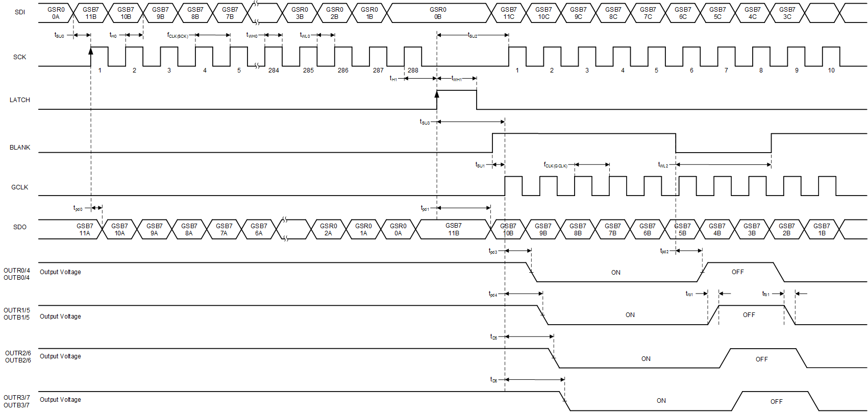
6.7 Switching Characteristics
over operating junction temperature range (unless otherwise noted)| PARAMETER | TEST CONDITIONS | MIN | TYP | MAX | UNIT | |
|---|---|---|---|---|---|---|
| tro0 | Rise time from 10% VSDO to 90% VSDO | 60 | ns | |||
| tro1 | Rise time from 10% VOUT to 90% VOUT | IOUT = 50 mA, SLEW_RATE = 0b | 200 | ns | ||
| tro2 | Rise time from 10% VOUT to 90% VOUT | IOUT = 50 mA, SLEW_RATE = 1b | 60 | 100 | 140 | ns |
| tfo0 | Fall time from 90% VSDO to 10% VSDO | 30 | ns | |||
| tfo1 | Fall time from 90% VOUT to 10% VOUT | IOUT = 50 mA , SLEW_RATE = 0b | 200 | ns | ||
| tfo2 | Fall time from 90% VOUT to 10% VOUT | IOUT = 50 mA, SLEW_RATE = 1b | 30 | 80 | 130 | ns |
| tpd0 | Propagation delay, SCK↑to SDO | 100 | 140 | 200 | ns | |
| tpd1 | Propagation delay, LATCH↑to SDO | 130 | 180 | 220 | ns | |
| tpd2 | Propagation delay, BLANK↓ to OUTR0, -G0, -B0, -R4, -G4, -B4 off | 10 | 120 | 260 | ns | |
| tpd3 | Propagation delay, GCLK↑ to OUTR0, -G0, -B0, -R4, -G4,-B4 on | 80 | 160 | 260 | ns | |
| tpd4 | Propagation delay, GCLK↑ to OUTR1, -G1, -B1, -R5, -G5, -B5 on | 120 | 200 | 330 | ns | |
| tpd5 | Propagation delay, GCLK↑ to OUTR2, -G2, -B2, -R6, -G6, -B6 on | 160 | 250 | 370 | ns | |
| tpd6 | Propagation delay, GCLK↑ to OUTR3, -G3, -B3, -R7, -G7, -B7 on | 190 | 280 | 400 | ns | |
| tpd7 | Propagation delay, LATCH↑ to VOUT | Changing by dot correction control (control data are 0Ch→72h or 72h→0Ch with upper DC range), BCR, -G, -B = FFh | 10 | 80 | 120 | ns |
| tpd8 | Propagation delay, LATCH↑ to VOUT | Changing by global brightness control (control data are 19h→E6h or E6h→19h with DCRn,-Gn, -Bn = 7Fh with upper DC range | 10 | 130 | 200 | ns |
| tpd9 | Propagation delay, LATCH↑ to APS register and APS_FLAG change | SINK_CURRENT = 0b | 5 | ns | ||
| tpd10 | Propagation delay, LATCH↑ to APS register and APS_FLAG change | SINK_CURRENT = 1b | 10 | ns | ||
| tpd11 | Propagation delay, LATCH↑ to LOD_LSD_FLAG change | No failure in LOD-LSD detector circuit | 24 | ns | ||
 Figure 1. Grayscale (GS) Data Write
  Figure 2. Function Control, Brightness Control, and Dot Correction Data (FC-BC-DC) Write
  Figure 3. Grayscale (GS) Data Read
  Figure 4. Status Information Data (SID) Read
  Figure 5. Adjacent-Pin-Short (APS) Check
  Figure 6. Negate Bit Toggle
  Figure 7. LOD_LSD Self-Test
  Figure 8. Function Control, Brightness Control, and Dot Correction Data (FC-BC-DC) Read
  Figure 9. ERROR Clear
  Figure 10. Global Reset
  Figure 11. 12-Bit Mode PWM Counter Without Auto-Repeat Mode
  Figure 12. 8-, 10-, 12-Bit Mode PWM Counter Without Auto-Repeat Mode
  Figure 13. 8-, 10-, 12-Bit Mode PWM Counter With Auto-Repeat Mode
  Figure 14. LOD-LSD Register Update Timing