SLASEJ5B October   2017  – January 2020 TLC6C5816-Q1

PRODUCTION DATA.  

  1. Features
  2. Applications
  3. Description
    1.     Typical Application Schematic
  4. Revision History
  5. Pin Configuration and Functions
    1.     Pin Functions
  6. Specifications
    1. 6.1 Absolute Maximum Ratings
    2. 6.2 ESD Ratings
    3. 6.3 Recommended Operating Conditions
    4. 6.4 Thermal Information
    5. 6.5 Electrical Characteristics
    6. 6.6 Timing Requirements
    7. 6.7 Switching Characteristics
    8. 6.8 Typical Characteristics
  7. Detailed Description
    1. 7.1 Overview
    2. 7.2 Functional Block Diagram
    3. 7.3 Feature Description
      1. 7.3.1 Device Enable (EN)
      2. 7.3.2 Gated Output (Gx)
      3. 7.3.3 Register Clear (CLR)
      4. 7.3.4 Open-Drain Outputs and Flexible Diagnostics Channel
        1. 7.3.4.1 Configurable Outputs
        2. 7.3.4.2 LED-Open Diagnostics
        3. 7.3.4.3 LED-Short Diagnostics
      5. 7.3.5 Thermal Shutdown
      6. 7.3.6 Command Error
      7. 7.3.7 Serial Communication Error
      8. 7.3.8 Error Feedback
      9. 7.3.9 Interface
        1. 7.3.9.1 Register Write
        2. 7.3.9.2 Register Read
        3. 7.3.9.3 Shift-Register Communication-Fault Detection
        4. 7.3.9.4 Clear Register
        5. 7.3.9.5 Register Clock
    4. 7.4 Device Functional Modes
      1. 7.4.1 Normal Operation
      2. 7.4.2 POR Reset
      3. 7.4.3 Standby Mode
    5. 7.5 Register Maps
    6. 7.6 Interface Registers
      1. 7.6.1 Configuration Register (Offset = 0h) [reset = 0h]
        1. Table 5. Configuration Register Field Descriptions
      2. 7.6.2 Fault Readback Register (Offset = 1h) [reset = 0h]
        1. Table 6. Fault Readback Register Field Descriptions
  8. Application and Implementation
    1. 8.1 Application Information
    2. 8.2 Typical Application
      1. 8.2.1 Design Requirements
      2. 8.2.2 Detailed Design Procedure
      3. 8.2.3 Application Curves
  9. Power Supply Recommendations
  10. 10Layout
    1. 10.1 Layout Guidelines
    2. 10.2 Layout Example
  11. 11Device and Documentation Support
    1. 11.1 Receiving Notification of Documentation Updates
    2. 11.2 Community Resources
    3. 11.3 Trademarks
    4. 11.4 Electrostatic Discharge Caution
    5. 11.5 Glossary
  12. 12Mechanical, Packaging, and Orderable Information

Package Options

Mechanical Data (Package|Pins)
Thermal pad, mechanical data (Package|Pins)
Orderable Information

Register Write

The TLC6C5816-Q1 device has a 24-bit configuration register. Data transfers through the shift registers on the rising edge of SRCK and latches into the storage registers on the rising edge of RCK. The first 8 data bits control the diagnostics channel configuration, and the following 16 data bits control 16 open-drain outputs independently.
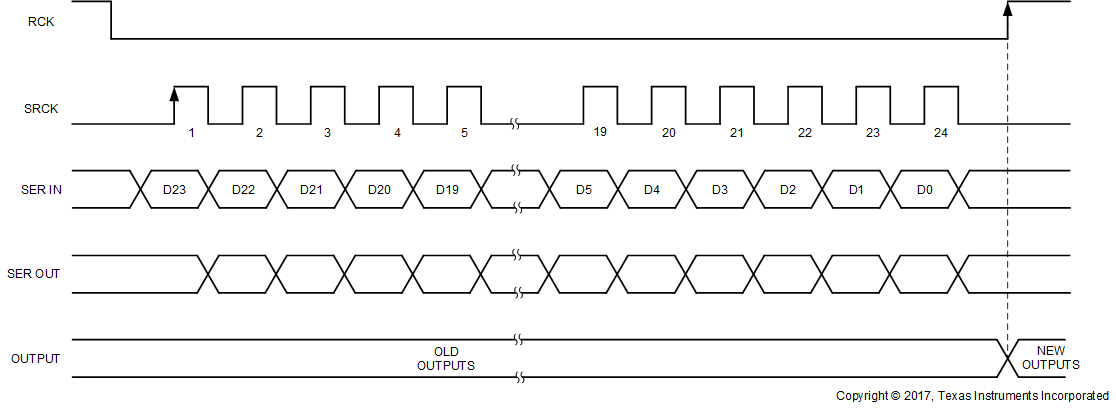
TLC6C5816-Q1 Data-Write-SLASEJ5.gifFigure 15. Register Write Timing Diagram

The DRAINn+1-DIAGn channel configuration is controlled by the DIAGn registers. These channels can be set to either open-drain output or diagnostics input mode. The TLC6C5816-Q1 device does not allow the user to set DRAINn+1 and DIAGn high at the same time, because the divider resistor for LED diagnostics can result in leakage current on the LED, which lights up the LED. If the DIAGn and DRAINn registers are set to high at the same time, the channel operates as an open-drain output instead of LED diagnostics, and a command error latches in the fault registers, which can be read back by the register readback function as explained in Register Read.