SLIS141C December 2012 – July 2016 TLC6C5912-Q1
PRODUCTION DATA.
- 1 Features
- 2 Applications
- 3 Description
- 4 Revision History
- 5 Pin Configuration and Functions
- 6 Specifications
- 7 Parameter Measurement Information
- 8 Detailed Description
- 9 Application and Implementation
- 10Power Supply Recommendations
- 11Layout
- 12Device and Documentation Support
- 13Mechanical, Packaging, and Orderable Information
Package Options
Mechanical Data (Package|Pins)
Thermal pad, mechanical data (Package|Pins)
Orderable Information
6 Specifications
6.1 Absolute Maximum Ratings
over operating free-air temperature range (unless otherwise noted)(1)| MIN | MAX | UNIT | |||
|---|---|---|---|---|---|
| VCC | Logic supply voltage | 8 | V | ||
| VI | Logic input-voltage | –0.3 | 8 | V | |
| VDS | Power DMOS drain-to-source voltage | 42 | V | ||
| Continuous total dissipation | See Thermal Information | ||||
| Operating ambient temperature (Top) | 125 | °C | |||
| TJ | Operating junction temperature | –40 | 150 | °C | |
| Tstg | Storage temperature | –55 | 165 | °C | |
(1) Stresses beyond those listed under Absolute Maximum Ratings may cause permanent damage to the device. These are stress ratings only, which do not imply functional operation of the device at these or any other conditions beyond those indicated under Recommended Operating Conditions. Exposure to absolute-maximum-rated conditions for extended periods may affect device reliability.
6.2 ESD Ratings
| VALUE | UNIT | |||||
|---|---|---|---|---|---|---|
| V(ESD) | Electrostatic discharge | Human body model (HBM), per AEC Q100-002(1) | ±2000 | V | ||
| Charged device model (CDM), per AEC Q100-011 | ±750 | |||||
(1) AEC Q100-002 indicates HBM stressing is done in accordance with the ANSI/ESDA/JEDEC JS-001 specification.
6.3 Recommended Operating Conditions
| MIN | MAX | UNIT | ||
|---|---|---|---|---|
| VCC | Supply voltage | 3 | 5.5 | V |
| VIH | High-level input voltage | 2.4 | V | |
| VIL | Low-level input voltage | 0.7 | V | |
| tsu | Setup time, SER IN high before SRCK↑ | 15 | ns | |
| th | Hold time, SER IN high after SRCK↑ | 15 | ns | |
| tw | Pulse duration | 40 | ns | |
| TC | Operating case temperature | –40 | 125 | °C |
6.4 Thermal Information
| THERMAL METRIC(1) | TLC6C5912-Q1 | UNIT | ||
|---|---|---|---|---|
| 20 PINS | ||||
| PW (TSSOP) | DW (SOIC) | |||
| RθJA | Junction-to-ambient thermal resistance | 114.8 | 81.2 | °C/W |
| RθJC(top) | Junction-to-case (top) thermal resistance | 44.1 | 45.4 | °C/W |
| RθJB | Junction-to-board thermal resistance | 61.3 | 49.1 | °C/W |
| ψJT | Junction-to-top characterization parameter | 4.7 | 17.5 | °C/W |
| ψJB | Junction-to-board characterization parameter | 60.8 | 48.6 | °C/W |
(1) For more information about traditional and new thermal metrics, see the Semiconductor and IC Package Thermal Metrics application report.
6.5 Electrical Characteristics
VCC = 5 V, TC = 25°C (unless otherwise noted)6.6 Switching Characteristics
VCC = 5 V, TJ = 25°C| PARAMETER | TEST CONDITIONS | MIN | TYP | MAX | UNIT | |
|---|---|---|---|---|---|---|
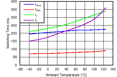
| tPLH | Propagation delay time, low-to-high-level output from G | CL = 30 pF, ID = 48 mA | 210 | ns | ||
| tPHL | Propagation delay time, high-to-low-level output from G | 75 | ns | |||
| tr | Rise time, drain output | 250 | ns | |||
| tf | Fall time, drain output | 200 | ns | |||
| tpd | Propagation delay time, SRCK↓ to SEROUT | CL = 30 pF, ID = 48 mA | 35 | ns | ||
| Tor | SEROUT rise time (10% to 90%) | CL = 30 pF | 20 | ns | ||
| Tof | SEROUT fall time (90% to 10%) | CL = 30 pF | 20 | ns | ||
| f(SRCK) | Serial clock frequency | CL = 30 pF, ID = 20 mA | 10 | MHz | ||
| TSRCK_WH | SRCK pulse duration, high | 30 | ns | |||
| TSRCK_WL | SRCK pulse duration, low | 30 | ns | |||
 Figure 1. SER IN to SER OUT Waveform
Figure 1 shows the SER IN to SER OUT waveform. The output signal appears on the falling edge of the shift register clock (SRCK) because there is a phase inverter at SER OUT (see Figure 2). As a result, it takes seven and a half periods of SRCK for data to transfer from SER IN to SER OUT.
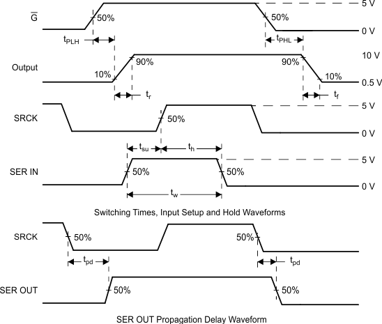 Figure 2. Switching Times and Voltage Waveforms
Figure 2 shows the switching times and voltage waveforms. Tests for all these parameters took place using the test circuit shown in Figure 12.
6.7 Typical Characteristics
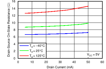
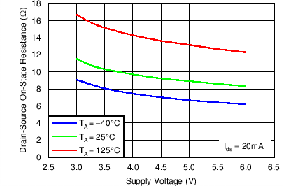
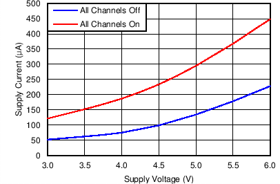
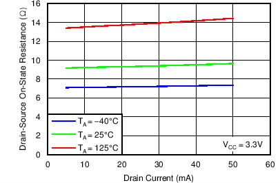
Conditions for Figure 5 and Figure 6: Single channel on; conditions for Figure 7, Figure 8, and Figure 9: All channels on.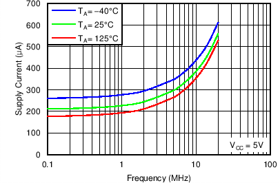
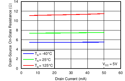
vs Drain Current
vs Drain Current
vs Drain Current
vs Drain Current
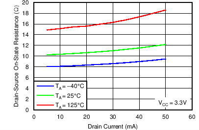
vs Drain Current
