SLIS142D December   2012  – September 2016 TLC6C598-Q1

PRODUCTION DATA.  

  1. Features
  2. Applications
  3. Description
  4. Revision History
  5. Pin Configuration and Functions
  6. Specifications
    1. 6.1 Absolute Maximum Ratings
    2. 6.2 ESD Ratings
    3. 6.3 Recommended Operating Conditions
    4. 6.4 Thermal Information
    5. 6.5 Electrical Characteristics
    6. 6.6 Timing Requirements
    7. 6.7 Switching Characteristics
    8. 6.8 Timing Waveforms
    9. 6.9 Typical Characteristics
  7. Parameter Measurement Information
  8. Detailed Description
    1. 8.1 Overview
    2. 8.2 Functional Block Diagram
    3. 8.3 Feature Description
      1. 8.3.1 Thermal Shutdown
      2. 8.3.2 Serial-In Interface
      3. 8.3.3 Clear Registers
      4. 8.3.4 Output Channels
      5. 8.3.5 Register Clock
      6. 8.3.6 Cascade Through SER OUT
      7. 8.3.7 Output Control
    4. 8.4 Device Functional Modes
      1. 8.4.1 Operation With VCC < 3 V
      2. 8.4.2 Operation With 5.5 V ≤ VCC ≤ 8 V
  9. Application and Implementation
    1. 9.1 Application Information
    2. 9.2 Typical Application
      1. 9.2.1 Design Requirements
      2. 9.2.2 Detailed Design Procedure
      3. 9.2.3 Application Curve
  10. 10Power Supply Recommendations
  11. 11Layout
    1. 11.1 Layout Guidelines
    2. 11.2 Layout Example
  12. 12Device and Documentation Support
    1. 12.1 Receiving Notification of Documentation Updates
    2. 12.2 Community Resources
    3. 12.3 Trademarks
    4. 12.4 Electrostatic Discharge Caution
    5. 12.5 Glossary
  13. 13Mechanical, Packaging, and Orderable Information
    1. 13.1 Package Option Addendum
      1. 13.1.1 Packaging Information
      2. 13.1.2 Tape and Reel Information

Package Options

Mechanical Data (Package|Pins)
Thermal pad, mechanical data (Package|Pins)

11 Layout

11.1 Layout Guidelines

There are no special layout requirement for the digital signal pins. The only requirement is placing the ceramic bypass capacitors near the corresponding pin.

Maximize the copper coverage on the PCB to increase the thermal conductivity of the board. The major heat-flow path from the package to the ambient is through the cooper on the PCB. Maximizing the copper coverage is extremely important when the design does not include heat sinks attached to the PCB on the other side of the package.

Add as many thermal vias as possible directly under the package ground pad to optimize the thermal conductivity of the board.

All thermal vias should be either plated shut or plugged and capped on both sides of the board to prevent solder voids. To ensure reliability and performance, the solder coverage should be at least 85%.

11.2 Layout Example
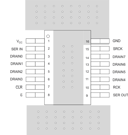
TLC6C598-Q1 Layout_SLIS142.gif Figure 16. TLC6C598-Q1 Example Layout