SLIS142D December   2012  – September 2016 TLC6C598-Q1

PRODUCTION DATA.  

  1. Features
  2. Applications
  3. Description
  4. Revision History
  5. Pin Configuration and Functions
  6. Specifications
    1. 6.1 Absolute Maximum Ratings
    2. 6.2 ESD Ratings
    3. 6.3 Recommended Operating Conditions
    4. 6.4 Thermal Information
    5. 6.5 Electrical Characteristics
    6. 6.6 Timing Requirements
    7. 6.7 Switching Characteristics
    8. 6.8 Timing Waveforms
    9. 6.9 Typical Characteristics
  7. Parameter Measurement Information
  8. Detailed Description
    1. 8.1 Overview
    2. 8.2 Functional Block Diagram
    3. 8.3 Feature Description
      1. 8.3.1 Thermal Shutdown
      2. 8.3.2 Serial-In Interface
      3. 8.3.3 Clear Registers
      4. 8.3.4 Output Channels
      5. 8.3.5 Register Clock
      6. 8.3.6 Cascade Through SER OUT
      7. 8.3.7 Output Control
    4. 8.4 Device Functional Modes
      1. 8.4.1 Operation With VCC < 3 V
      2. 8.4.2 Operation With 5.5 V ≤ VCC ≤ 8 V
  9. Application and Implementation
    1. 9.1 Application Information
    2. 9.2 Typical Application
      1. 9.2.1 Design Requirements
      2. 9.2.2 Detailed Design Procedure
      3. 9.2.3 Application Curve
  10. 10Power Supply Recommendations
  11. 11Layout
    1. 11.1 Layout Guidelines
    2. 11.2 Layout Example
  12. 12Device and Documentation Support
    1. 12.1 Receiving Notification of Documentation Updates
    2. 12.2 Community Resources
    3. 12.3 Trademarks
    4. 12.4 Electrostatic Discharge Caution
    5. 12.5 Glossary
  13. 13Mechanical, Packaging, and Orderable Information
    1. 13.1 Package Option Addendum
      1. 13.1.1 Packaging Information
      2. 13.1.2 Tape and Reel Information

Package Options

Mechanical Data (Package|Pins)
Thermal pad, mechanical data (Package|Pins)

7 Parameter Measurement Information

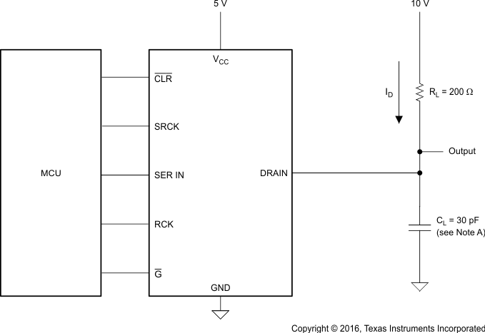
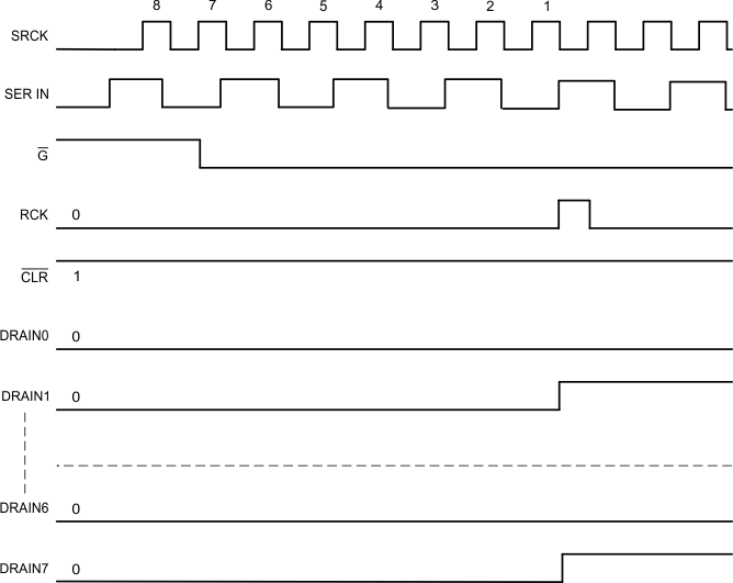
Figure 11 and Figure 12 show the resistive-load test circuit and voltage waveforms. One can see from Figure 12 that with G held low and CLR held high, the status of each drain changes on the rising edge of the register clock, indicating the transfer of data to the output buffers at that time.
TLC6C598-Q1 Res-Load_Test_SLIS141.gif
A. CL includes probe and jig capacitance.
Figure 11. Resistive-Load Test Circuit
TLC6C598-Q1 Voltage_Waveforms_SLIS142.gif Figure 12. Voltage Waveforms