SLVS647I August 2006 – November 2014 TLE4275-Q1
UNLESS OTHERWISE NOTED, this document contains PRODUCTION DATA.
- 1 Features
- 2 Applications
- 3 Description
- 4 Revision History
- 5 Pin Configuration and Functions
- 6 Specifications
- 7 Parameter Measurement Information
- 8 Detailed Description
- 9 Application and Implementation
- 10Power Supply Recommendations
- 11Layout
- 12Device and Documentation Support
- 13Mechanical, Packaging, and Orderable Information
Package Options
Refer to the PDF data sheet for device specific package drawings
Mechanical Data (Package|Pins)
- KTT|5
- PWP|20
- KVU|5
Thermal pad, mechanical data (Package|Pins)
Orderable Information
8 Detailed Description
8.1 Overview
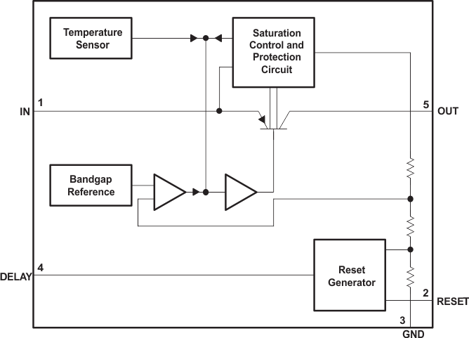
The TLE4275-Q1 device is a monolithic integrated low-dropout voltage regulator offered in a 5-pin TO package. The device regulates an input voltage up to 45 V to VOUT = 5 V (typical). The device can drive loads up to 450 mA and is short circuit proof. At over temperature, the incorporated temperature protection turns off the TLE4275-Q1 device. The device generates a reset signal for an output voltage, VOUT,rt, of 4.65 V (typical). By the use of an external delay capacitor, one can program the reset delay time.
8.2 Functional Block Diagram

8.3 Feature Description
8.3.1 Regulated Output (OUT)
The OUT terminal is the regulated 5-V output. The output has current limitation. During initial power up, the regulator has a soft start incorporated to control the initial current through the pass element. In the event that the regulator drops out of regulation, the output tracks the input minus a drop based on the load current.
8.3.2 Power-On-Reset (RESET)
The power-on-reset is an output with an external pull up resistor to the regulated supply. The reset output remains low until the regulated VO exceeds approximately 4.65 V and the power-on-reset delay has expired.
8.3.3 Reset Delay Timer (DELAY)
An external capacitor on this terminal sets the timer delay before the reset terminal is asserted high. The constant output current charges an external capacitor until the voltage exceeds a threshold to trip an internal comparator. The reset pulse delay time td, is defined with the charge time of an external capacitor DELAY.

8.4 Device Functional Modes
8.4.1 Low-Voltage Tracking
At low input voltages, the regulator drops out of regulation and the output voltage tracks input minus a voltage based on the load current (IO) and switch resistance (R(SW)). This allows for a smaller input capacitor and can possibly eliminate the need of using a boost convertor during cold-crank conditions.