SLLSFF6 September 2021 TLIN1024A-Q1
PRODUCTION DATA
- 1 Features
- 2 Applications
- 3 Description
- 4 Revision History
- 5 Description (Continued)
- 6 Pin Configuration and Functions
- 7 Specifications
- 8 Parameter Measurement Information
-
9 Detailed Description
- 9.1 Overview
- 9.2 Functional Block Diagram
- 9.3
Feature Description
- 9.3.1 LIN (Local Interconnect Network) Bus
- 9.3.2 TXD (Transmit Input and Output)
- 9.3.3 RXD (Receive Output)
- 9.3.4 VSUP1/2 (Supply Voltage)
- 9.3.5 GND1/2 (Ground)
- 9.3.6 EN (Enable Input)
- 9.3.7 Protection Features
- 9.3.8 TXD Dominant Time Out (DTO)
- 9.3.9 Bus Stuck Dominant System Fault: False Wake-Up Lockout
- 9.3.10 Thermal Shutdown
- 9.3.11 Under Voltage on VSUP
- 9.3.12 Unpowered Device and LIN Bus
- 9.4 Device Functional Modes
- 10Application and Implementation
- 11Power Supply Recommendations
- 12Layout
- 13Device and Documentation Support
- 14Mechanical, Packaging, and Orderable Information
Package Options
Mechanical Data (Package|Pins)
- RGY|24
Thermal pad, mechanical data (Package|Pins)
- RGY|24
Orderable Information
9.4 Device Functional Modes
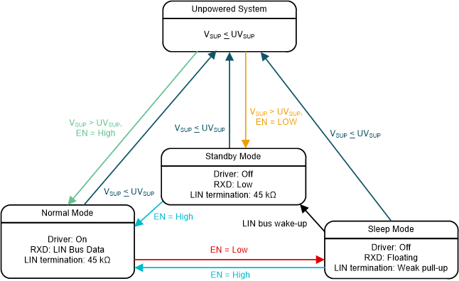
The TLIN1024A-Q1 has three functional modes of operation, normal, sleep, and standby. The next sections describe these modes as well as how the device moves between the different modes. Figure 9-4 graphically shows the relationship while Table 9-1 shows the state of pins.
Table 9-1 Operating Modes
| MODE | ENx | RXDx | LIN BUS TERMINATION | TRANSMITTER | COMMENT |
|---|---|---|---|---|---|
| Sleep | Low | Floating | Weak Current Pull-up | Off | |
| Standby | Low | Low | 45 kΩ (typical) | Off | Wake-up event detected, waiting on MCU to set EN |
| Normal | High | LINx Bus Data | 45 kΩ (typical) | On | LINx transmission up to 20 kbps |
 Figure 9-4 Operating
State Diagram