SLLSFF6 September 2021 TLIN1024A-Q1
PRODUCTION DATA
- 1 Features
- 2 Applications
- 3 Description
- 4 Revision History
- 5 Description (Continued)
- 6 Pin Configuration and Functions
- 7 Specifications
- 8 Parameter Measurement Information
-
9 Detailed Description
- 9.1 Overview
- 9.2 Functional Block Diagram
- 9.3
Feature Description
- 9.3.1 LIN (Local Interconnect Network) Bus
- 9.3.2 TXD (Transmit Input and Output)
- 9.3.3 RXD (Receive Output)
- 9.3.4 VSUP1/2 (Supply Voltage)
- 9.3.5 GND1/2 (Ground)
- 9.3.6 EN (Enable Input)
- 9.3.7 Protection Features
- 9.3.8 TXD Dominant Time Out (DTO)
- 9.3.9 Bus Stuck Dominant System Fault: False Wake-Up Lockout
- 9.3.10 Thermal Shutdown
- 9.3.11 Under Voltage on VSUP
- 9.3.12 Unpowered Device and LIN Bus
- 9.4 Device Functional Modes
- 10Application and Implementation
- 11Power Supply Recommendations
- 12Layout
- 13Device and Documentation Support
- 14Mechanical, Packaging, and Orderable Information
Package Options
Mechanical Data (Package|Pins)
- RGY|24
Thermal pad, mechanical data (Package|Pins)
- RGY|24
Orderable Information
10.2.2 Application Curves
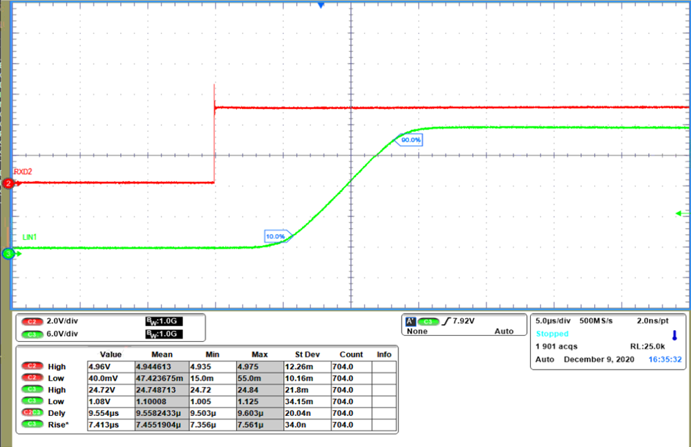
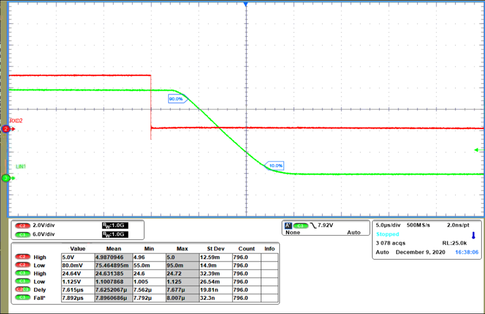
Figure 10-2 and Figure 10-3 show the propagation delay from the TXD pin to the LIN pin for both dominant to recessive and recessive to dominant edges. Waveforms are for 1 channel of the device configured in commander mode with external pull-up resistor (1 kΩ) and 680 pF bus capacitance.
 Figure 10-2 Dominant to
Recessive Propagation
 Figure 10-3 Recessive to
Dominant Propagation