SLLSFK7A March 2021 – April 2022 TLIN2021A-Q1
PRODMIX
- 1 Features
- 2 Applications
- 3 Description
- 4 Revision History
- 5 Description (continued)
- 6 Pin Configuration and Functions
- 7 Specification
- 8 Parameter Measurement Information
-
9 Detailed Description
- 9.1 Overview
- 9.2 Functional Block Diagram
- 9.3 Feature Description
- 9.4 Device Functional Modes
- 10Application Information Disclaimer
- 11Power Supply Recommendations
- 12Layout
- 13Device and Documentation Support
- 14Mechanical, Packaging, and Orderable Information
Package Options
Mechanical Data (Package|Pins)
Thermal pad, mechanical data (Package|Pins)
- DRB|8
Orderable Information
3 Description
The TLIN2021A-Q1 is a local interconnect network (LIN) physical layer transceiver. LIN is a low-speed universal asynchronous receiver transmitter (UART) communication protocol that supports automotive in-vehicle networking.
The TLIN2021A-Q1 transmitter supports data rates up to 20 kbps. The transceiver controls the state of the LIN bus via the TXD pin and reports the state of the bus on its open-drain RXD output pin. The device has a current-limited wave-shaping driver to reduce electromagnetic emissions (EME).
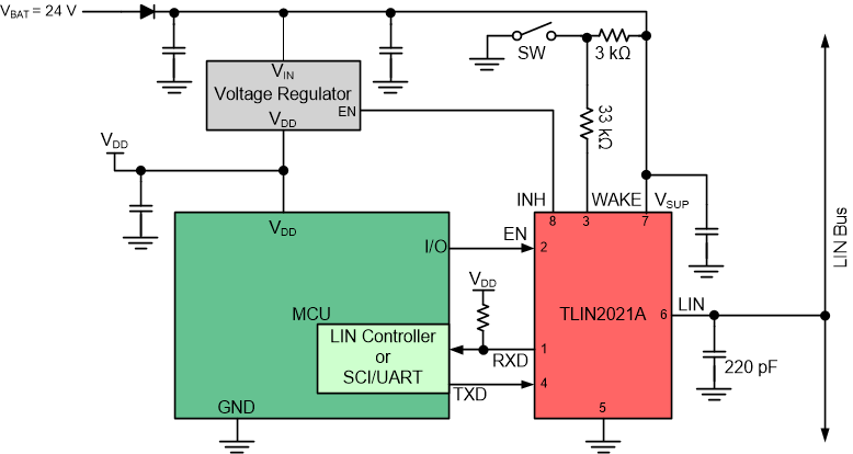
The TLIN2021A-Q1 is designed to support 12-V and 24-V applications with a wide input voltage operating range. The device supports low-power sleep mode, as well as wake-up from low-power mode through wake over LIN, the WAKE pin, or the EN pin. The device allows for system-level reductions in battery current consumption by selectively enabling the various power supplies that can be present on a node through the device INH output pin.
| PART NUMBER | PACKAGE(1) | BODY SIZE (NOM) |
|---|---|---|
| TLIN2021A | SOIC (D) (8)(2) | 4.90 mm x 3.91 mm |
| VSON (DRB) (8) | 3.00 mm x 3.00 mm | |
| SOT23 (DDF) (8)(2) | 2.90 mm x 1.60 mm |
 Simplified Responder Node Schematic