SLLSFK7A March   2021  – April 2022 TLIN2021A-Q1

PRODMIX  

  1. Features
  2. Applications
  3. Description
  4. Revision History
  5. Description (continued)
  6. Pin Configuration and Functions
  7. Specification
    1. 7.1 Absolute Maximum Ratings
    2. 7.2 ESD Ratings
    3. 7.3 ESD Ratings - IEC Specification
    4. 7.4 Thermal Information
    5. 7.5 Recommended Operating Conditions
    6. 7.6 Power Supply Characteristics
    7. 7.7 Electrical Characteristics
    8. 7.8 AC Switching Characteristics
    9. 7.9 Typical Curves
  8. Parameter Measurement Information
  9. Detailed Description
    1. 9.1 Overview
    2. 9.2 Functional Block Diagram
    3. 9.3 Feature Description
      1. 9.3.1  LIN
        1. 9.3.1.1 LIN Transmitter Characteristics
        2. 9.3.1.2 LIN Receiver Characteristics
          1. 9.3.1.2.1 Termination
      2. 9.3.2  TXD
      3. 9.3.3  RXD
      4. 9.3.4  VSUP
      5. 9.3.5  GND
      6. 9.3.6  EN
      7. 9.3.7  WAKE
      8. 9.3.8  INH
      9. 9.3.9  Local Faults
      10. 9.3.10 TXD Dominant Time-Out (DTO)
      11. 9.3.11 Bus Stuck Dominant System Fault: False Wake-Up Lockout
      12. 9.3.12 Thermal Shutdown
      13. 9.3.13 Under Voltage on VSUP
      14. 9.3.14 Unpowered Device
    4. 9.4 Device Functional Modes
      1. 9.4.1 Normal Mode
      2. 9.4.2 Sleep Mode
      3. 9.4.3 Standby Mode
      4. 9.4.4 Wake-Up Events
        1. 9.4.4.1 Local Wake-Up (LWU) via WAKE Input Terminal
        2. 9.4.4.2 Wake-Up Request (RXD)
  10. 10Application Information Disclaimer
    1. 10.1 Application Information
    2. 10.2 Typical Application
      1. 10.2.1 Design Requirements
      2. 10.2.2 Detailed Design Procedures
        1. 10.2.2.1 Normal Mode Application Note
        2. 10.2.2.2 TXD Dominant State Time-Out Application Note
        3. 10.2.2.3 Standby Mode Application Note
      3. 10.2.3 Application Curves
  11. 11Power Supply Recommendations
  12. 12Layout
    1. 12.1 Layout Guidelines
    2. 12.2 Layout Example
  13. 13Device and Documentation Support
    1. 13.1 Documentation Support
    2. 13.2 Receiving Notification of Documentation Updates
    3. 13.3 Support Resources
    4. 13.4 Trademarks
    5. 13.5 Electrostatic Discharge Caution
    6. 13.6 Glossary
  14. 14Mechanical, Packaging, and Orderable Information

Package Options

Mechanical Data (Package|Pins)
Thermal pad, mechanical data (Package|Pins)
Orderable Information

Device Functional Modes

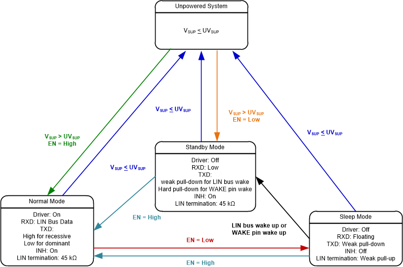
The TLIN2021A-Q1 has three functional modes of operation: normal, sleep, and standby. The next sections describe these modes and how the device transitions between the different modes. Figure 9-4 graphically shows the relationship while Table 9-1 shows the state of pins.

Table 9-1 Operating Modes
MODEENTXDRXDINHLIN BUS
TERMINATION
TRANSMITTERCOMMENT
SleepLowWeak pull-downFloatingFloatingWeak current pull-upOff
StandbyLowWeak pull-down if LIN bus wake-up; Strong pull-down if a local wake-up event (WAKE pin)LowHigh45-kΩOffWake-up event detected,
waiting on MCU to set EN
NormalHighHigh: recessive state
Low: dominant state
LIN Bus DataHigh45-kΩOnLIN transmission up to 20 kbps
GUID-D8D7F1B3-C448-494F-9552-423D639FC384-low.gifFigure 9-4 Operating State Diagram