SLLSEY6G October   2017  – February 2024 TLIN2029-Q1

PRODUCTION DATA  

  1.   1
  2. Features
  3. Applications
  4. Description
  5. Pin Configuration and Functions
  6. Specifications
    1. 5.1 Absolute Maximum Ratings
    2. 5.2 ESD Ratings
    3. 5.3 ESD Ratings - IEC
    4. 5.4 Thermal Information
    5. 5.5 Recommended Operating Conditions
    6. 5.6 Electrical Characteristics
    7. 5.7 Switching Characteristics
    8. 5.8 Timing Requirements
  7. Parameter Measurement Information
  8. Detailed Description
    1. 7.1 Overview
    2. 7.2 Functional Block Diagram
    3. 7.3 Feature Description
      1. 7.3.1  LIN (Local Interconnect Network) Bus
        1. 7.3.1.1 LIN Transmitter Characteristics
        2. 7.3.1.2 LIN Receiver Characteristics
          1. 7.3.1.2.1 Termination
      2. 7.3.2  TXD (Transmit Input and Output)
      3. 7.3.3  RXD (Receive Output)
      4. 7.3.4  VSUP (Supply Voltage)
      5. 7.3.5  GND (Ground)
      6. 7.3.6  EN (Enable Input)
      7. 7.3.7  Protection Features
      8. 7.3.8  TXD Dominant Time Out (DTO)
      9. 7.3.9  Bus Stuck Dominant System Fault: False Wake-Up Lockout
      10. 7.3.10 Thermal Shutdown
      11. 7.3.11 Under Voltage on VSUP
      12. 7.3.12 Unpowered Device and LIN Bus
    4. 7.4 Device Functional Modes
      1. 7.4.1 Normal Mode
      2. 7.4.2 Sleep Mode
      3. 7.4.3 Standby Mode
      4. 7.4.4 Wake-Up Events
        1. 7.4.4.1 Wake-Up Request (RXD)
        2. 7.4.4.2 Mode Transitions
  9. Application and Implementation
    1. 8.1 Application Information
    2. 8.2 Typical Application
      1. 8.2.1 Design Requirements
      2. 8.2.2 Detailed Design Procedures
        1. 8.2.2.1 Normal Mode Application Note
        2. 8.2.2.2 Standby Mode Application Note
          1. 8.2.2.2.1 TXD Dominant State Timeout Application Note
      3. 8.2.3 Application Curves
    3. 8.3 Power Supply Recommendations
    4. 8.4 Layout
      1. 8.4.1 Layout Guidelines
      2. 8.4.2 Layout Example
  10. Device and Documentation Support
    1. 9.1 Documentation Support
      1. 9.1.1 Related Documentation
    2. 9.2 Receiving Notification of Documentation Updates
    3. 9.3 Support Resources
    4. 9.4 Trademarks
    5. 9.5 Electrostatic Discharge Caution
    6. 9.6 Glossary
  11. 10Revision History
  12. 11Mechanical, Packaging, and Orderable Information

Package Options

Mechanical Data (Package|Pins)
Thermal pad, mechanical data (Package|Pins)
Orderable Information

Application Curves

The below figures show the propagation delay from the TXD pin to the LIN pin for both dominant to recessive and recessive to dominant stated under lightly loaded conditions.

GUID-EED971E9-EA50-4F32-AF55-11FA1374BA9A-low.pngFigure 8-2 Recessive to Dominant Propagation
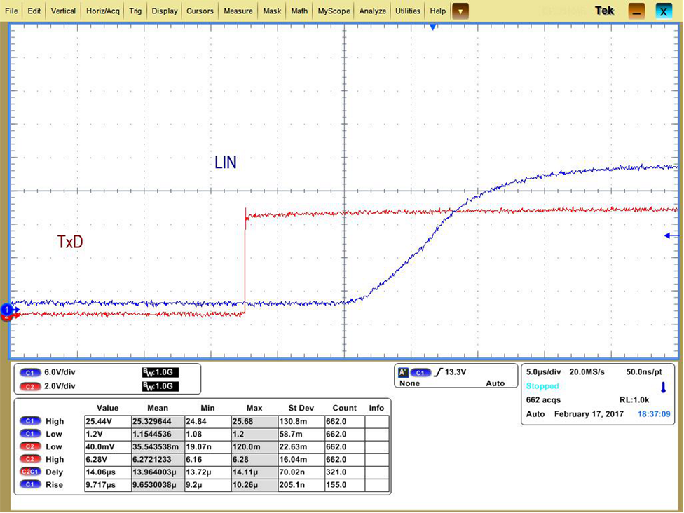
GUID-302D121F-17DF-4E5E-BB43-C89DA3B0ECDC-low.pngFigure 8-3 Dominant to Recessive Propagation