SLLSEF8C August 2013 – November 2014 TLK111
PRODUCTION DATA.
- 1 Introduction
- 2 Pin Descriptions
-
3 Hardware Configuration
- 3.1 Bootstrap Configuration
- 3.2 Power Supply Configuration
- 3.3 IO Pins Hi-Z State During Reset
- 3.4 Auto-Negotiation
- 3.5 Auto-MDIX
- 3.6 PHY Address
- 3.7 MII Isolate Mode
- 3.8 Software Strapping Mode
- 3.9 LED Interface
- 3.10 Multi-Configurable LED (MLED)
- 3.11 Loopback Functionality
- 3.12 BIST
- 3.13 Cable Diagnostics
- 4 Interfaces
-
5 Architecture
- 5.1 100Base-TX Transmit Path
- 5.2
100Base-TX Receive Path
- 5.2.1 Analog Front End
- 5.2.2 Adaptive Equalizer
- 5.2.3 Baseline Wander Correction
- 5.2.4 NRZI and MLT-3 Decoding
- 5.2.5 Descrambler
- 5.2.6 5B/4B Decoder and Nibble Alignment
- 5.2.7 Timing Loop and Clock Recovery
- 5.2.8 Phase-Locked Loops (PLL)
- 5.2.9 Link Monitor
- 5.2.10 Signal Detect
- 5.2.11 Bad SSD Detection
- 5.3 10Base-T Receive Path
- 5.4 Auto Negotiation
- 5.5 Link Down Functionality
- 5.6 IEEE 1588 Precision Timing Protocol Support
- 6 Reset and Power Down Operation
- 7 Design Guidelines
-
8 Register Block
- 8.1
Register Definition
- 8.1.1 Basic Mode Control Register (BMCR)
- 8.1.2 Basic Mode Status Register (BMSR)
- 8.1.3 PHY Identifier Register 1 (PHYIDR1)
- 8.1.4 PHY Identifier Register 2 (PHYIDR2)
- 8.1.5 Auto-Negotiation Advertisement Register (ANAR)
- 8.1.6 Auto-Negotiation Link Partner Ability Register (ANLPAR) (BASE Page)
- 8.1.7 Auto-Negotiate Expansion Register (ANER)
- 8.1.8 Auto-Negotiate Next Page Transmit Register (ANNPTR)
- 8.1.9 Auto-Negotiation Link Partner Ability Next Page Register (ANLNPTR)
- 8.1.10 Software Strap Control register 1 (SWSCR1)
- 8.1.11 Software Strap Control register 2 (SWSCR2)
- 8.1.12 Software Strap Control Register 3 (SWSCR3)
- 8.1.13 Extended Register Addressing
- 8.1.14 Fast Link Down Status Register
- 8.1.15 PHY Status Register (PHYSTS)
- 8.1.16 PHY Specific Control Register (PHYSCR)
- 8.1.17 MII Interrupt Status Register 1 (MISR1)
- 8.1.18 MII Interrupt Status Register 2 (MISR2)
- 8.1.19 False Carrier Sense Counter Register (FCSCR)
- 8.1.20 Receiver Error Counter Register (RECR)
- 8.1.21 BIST Control Register (BISCR)
- 8.1.22 RMII Control and Status Register (RCSR)
- 8.1.23 LED Control Register (LEDCR)
- 8.1.24 PHY Control Register (PHYCR)
- 8.1.25 10Base-T Status/Control Register (10BTSCR)
- 8.1.26 BIST Control and Status Register 1 (BICSR1)
- 8.1.27 BIST Control and Status Register2 (BICSR2)
- 8.2 Cable Diagnostic Control Register (CDCR)
- 8.3 PHY Reset Control Register (PHYRCR)
- 8.4 Multi LED Control register (MLEDCR)
- 8.5 IEEE1588 Precision Timing Pin Select (PTPPSEL)
- 8.6 IEEE1588 Precision Timing Configuration (PTPCFG)
- 8.7 TX_CLK Phase Shift Register (TXCPSR)
- 8.8 Power Back Off Control Register (PWRBOCR)
- 8.9 Voltage Regulator Control Register (VRCR)
- 8.10
Cable Diagnostic Configuration/Result Registers
- 8.10.1 ALCD Control and Results 1 (ALCDRR1)
- 8.10.2 Cable Diagnostic Specific Control Registers (CDSCR1 - CDSCR4)
- 8.10.3 Cable Diagnostic Location Results Register 1 (CDLRR1)
- 8.10.4 Cable Diagnostic Location Results Register 2 (CDLRR2)
- 8.10.5 Cable Diagnostic Location Results Register 3 (DDLRR3)
- 8.10.6 Cable Diagnostic Location Results Register 4 (CDLRR4)
- 8.10.7 Cable Diagnostic Location Results Register 5 (CDLRR5)
- 8.10.8 Cable Diagnostic Amplitude Results Register 1 (CDARR1)
- 8.10.9 Cable Diagnostic Amplitude Results Register 2 (CDARR2)
- 8.10.10 Cable Diagnostic Amplitude Results Register 3 (CDARR3)
- 8.10.11 Cable Diagnostic Amplitude Results Register 4 (CDARR4)
- 8.10.12 Cable Diagnostic Amplitude Results Register 5 (CDARR5)
- 8.10.13 Cable Diagnostic General Results Register (CDGRR)
- 8.10.14 ALCD Control and Results 2 (ALCDRR2)
- 8.10.15 ALCD Control and Results 3 (ALCDRR3)
- 8.1
Register Definition
-
9 Electrical Specifications
- 9.1 Absolute Maximum Ratings
- 9.2 Handling Ratings
- 9.3 Recommended Operating ConditionsRedundant row "Power dissipation 200 mW"
- 9.4 48-Pin Industrial Device Thermal Characteristics
- 9.5 48-Pin Extended Temperature (125°C) Device Thermal Characteristics
- 9.6 DC Characteristics, VDD_IO DC Characteristics, SD_IN
- 9.7 DC Characteristics
- 9.8 Power Supply Characteristics
- 9.9
AC Specifications
- 9.9.1 Power Up Timing
- 9.9.2 Reset Timing
- 9.9.3 MII Serial Management Timing
- 9.9.4 100Mb/s MII Transmit Timing
- 9.9.5 100Mb/s MII Receive Timing
- 9.9.6 100Base-TX Transmit Packet Latency Timing
- 9.9.7 100Base-TX Transmit Packet Deassertion Timing
- 9.9.8 100Base-TX Transmit Timing (tR/F and Jitter)
- 9.9.9 100Base-TX Receive Packet Latency Timing
- 9.9.10 100Base-TX Receive Packet Deassertion Timing
- 9.9.11 10Mbs MII Transmit Timing
- 9.9.12 10Mb/s MII Receive Timing
- 9.9.13 10Base-T Transmit Timing (Start of Packet)
- 9.9.14 10Base-T Transmit Timing (End of Packet)
- 9.9.15 10Base-T Receive Timing (Start of Packet)
- 9.9.16 10Base-T Receive Timing (End of Packet)
- 9.9.17 10Mb/s Jabber Timing
- 9.9.18 10Base-T Normal Link Pulse Timing
- 9.9.19 Auto-Negotiation Fast Link Pulse (FLP) Timing
- 9.9.20 100Base-TX Signal Detect Timing
- 9.9.21 100Mbs Loopback Timing
- 9.9.22 10Mbs Internal Loopback Timing
- 9.9.23 RMII Transmit Timing
- 9.9.24 RMII Receive Timing
- 9.9.25 Isolation Timing
- 9.9.26 25MHz_OUT Clock Timing
- 10Revision History, Revision A
Package Options
Mechanical Data (Package|Pins)
- PT|48
Thermal pad, mechanical data (Package|Pins)
Orderable Information
1 Introduction
1.1 Features
- Fully Pin Compatible with the TLK110 Device
- Low Power Consumption:
- Single Supply: <205mW PHY, 275mW with Center Tap (Typical)
- Dual Supplies: <126mW PHY, 200mW with Center Tap (Typical)
- Programmable Power Back Off to reduce PHY power up to 20% in systems with shorter cables
- IEEE 1588 SFD indication enables time stamping by a controller or processor
- Low deterministic latency supports IEEE1588 implementation
- Cable Diagnostics
- Programmable Fast Link Down Modes, <10µs reaction time
- Variable I/O voltage range: 1.8V to 3.3V
- 3.3-V MAC Interface
- Fixed TX Clock to XI, with programmable phase shift
- Auto-MDIX for 10/100Mbs
- Energy Detection Mode
- 25 MHz Clock Out
- MII and RMII Capabilities
- IEEE 802.3u MII
- IEEE 802.3u Auto-Negotiation and Parallel Detection
- Error-Free 100Base-T Operation up to 150 Meters Under Typical Conditions
- Error-Free 10Base-T Operation up to 300 Meters Under Typical Conditions
- Serial Management Interface
- IEEE 802.3u ENDEC, 10Base-T Transceivers and Filters
- IEEE 802.3u PCS, 100Base-TX Transceivers
- IEEE 1149.1 JTAG
- Integrated ANSI X3.263 Compliant TP-PMD Physical Sublayer with Adaptive Equalization and Baseline Wander Compensation
- Programmable LED Support Link, 10/100Mbs Mode, Activity, and Collision Detect
- 10/100Mbs Packet BIST (Built in Self Test)
- HBM ESD protection on RD± and TD± of 16kV
- 48-pin LQFP Package (7mm) × (7mm)
1.2 Applications
1.3 Description
The TLK111 is a single-port Ethernet PHY for 10Base-T and 100Base TX signaling. This device integrates all the physical-layer functions needed to transmit and receive data on standard twisted-pair cables. The TLK111 supports the standard Media Independent Interface (MII) and Reduced Media Independent Interface (RMII) for direct connection to a Media Access Controller (MAC).
The TLK111 is designed for power-supply flexibility, and can operate with a single 3.3V power supply or with combinations of 3.3V and 1.55V power supplies for reduced power operation.
The TLK111 uses mixed-signal processing to perform equalization, data recovery, and error correction to achieve robust operation over CAT 5 twisted-pair wiring. This device not only meets the requirements of IEEE 802.3, but maintains high margins in terms of cross-talk and alien noise.
The TLK111 Ethernet PHY has a special Power Back Off mode to conserve power in systems with relatively short cables. This mode provides the flexibility to reduce system power when the system is not required to drive the standard IEEE 802.3 100m cable length, or the extended 150m, error-free cable reach of the TLK111. For more detail, see application note SLLA328.
1.4 Functional Block Diagrams
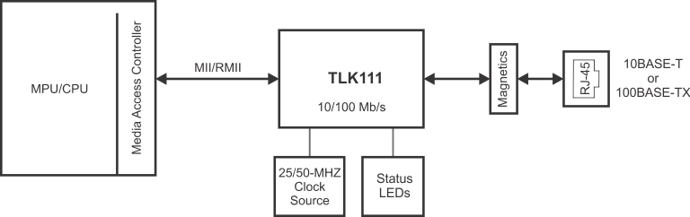
 Figure 1-1 TLK111 Functional Block Diagram