SGLS307Q July 2006 – August 2024 TLK2711-SP
PRODUCTION DATA
- 1
- 1 Features
- 2 Applications
- 3 Description
- 4 Pin Configuration and Functions
-
5 Specifications
- 5.1 Absolute Maximum Ratings
- 5.2 ESD Ratings
- 5.3 Recommended Operating Conditions
- 5.4 Thermal Information
- 5.5 TTL Input Electrical Characteristics
- 5.6 Transmitter/Receiver Electrical Characteristics
- 5.7 Reference Clock (TXCLK) Timing Requirements
- 5.8 TTL Output Switching Characteristics
- 5.9 Typical Characteristics
-
6 Detailed Description
- 6.1 Overview
- 6.2 Functional Block Diagram
- 6.3
Feature Description
- 6.3.1 Transmit Interface
- 6.3.2 Transmit Data Bus
- 6.3.3 Data Transmission Latency
- 6.3.4 8-Bit/10-Bit Encoder
- 6.3.5 Pseudo-Random Bit Stream (PRBS) Generator
- 6.3.6 Parallel to Serial
- 6.3.7 High-Speed Data Output
- 6.3.8 Receive Interface
- 6.3.9 Receive Data Bus
- 6.3.10 Data Reception Latency
- 6.3.11 Serial to Parallel
- 6.3.12 Comma Detect and 8-Bit/10-Bit Decoding
- 6.3.13 LOS Detection
- 6.3.14 PRBS Verification
- 6.3.15 Reference Clock Input
- 6.3.16 Operating Frequency Range
- 6.3.17 Testability
- 6.3.18 Loopback Testing
- 6.3.19 BIST
- 6.3.20 Power-On Reset
- 6.4 Device Functional Modes
- 7 Application and Implementation
- 8 Device and Documentation Support
- 9 Revision History
- 10Mechanical, Packaging, and Orderable Information
Package Options
Mechanical Data (Package|Pins)
- HFG|68
Thermal pad, mechanical data (Package|Pins)
Orderable Information
3 Description
The TLK2711-SP is a member of the WizardLink transceiver family of multigigabit transceivers, intended for use in ultra-high-speed bidirectional point-to-point data transmission systems. The TLK2711-SP supports an effective serial interface speed of 1.6Gbps to 2.5Gbps, providing up to 2Gbps of data bandwidth.
The primary application of the TLK2711-SP is to provide high-speed I/O data channels for point-to-point baseband data transmission over controlled impedance media of approximately 50Ω. The transmission media can be printed circuit board, copper cables, or fiber-optic cable. The maximum rate and distance of data transfer is dependent upon the attenuation characteristics of the media and the noise coupling to the environment.
This device can also be used to replace parallel data transmission architectures by providing a reduction in the number of traces, connector pins, and transmit/receive pins. Parallel data loaded into the transmitter is delivered to the receiver over a serial channel, which can be a coaxial copper cable, a controlled impedance backplane, or an optical link. It is then reconstructed into its original parallel format. It offers significant power and cost savings over parallel solutions, as well as scalability for higher data rates in the future.
The TLK2711-SP performs parallel-to-serial and serial-to-parallel data conversion. The clock extraction functions as a physical layer (PHY) interface device. The serial transceiver interface operates at a maximum speed of 2.5Gbps. The transmitter latches 16-bit parallel data at a rate based on the supplied reference clock (TXCLK). The 16-bit parallel data is internally encoded into 20 bits using an 8-bit/10-bit (8b/10b) encoding format. The resulting 20-bit word is then transmitted differentially at 20× the reference clock (TXCLK) rate. The receiver section performs the serial-to-parallel conversion on the input data, synchronizing the resulting 20-bit wide parallel data to the recovered clock (RXCLK). It then decodes the 20-bit wide data using the 8-bit/10-bit decoding format resulting in 16 bits of parallel data at the receive data pins (RXD0–RXD15). The outcome is an effective data payload of 1.28Gbps to 2Gbps (16 bits data × the frequency).
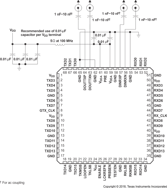
The TLK2711-SP is available in a 68-pin ceramic nonconductive tie-bar package (HFG).
The errata noted in the commercial TLK2711 device titled Errata to the TLK2711, 1.6-to-2.7 GBPS Transceiver Data Sheet– PLL False Lock Problem does not apply to the TLK2711-SP device. The TLK2711-SP is functionally equivalent to the TLK2711A commercial device.
The TLK2711-SP provides an internal loopback capability for self-test purposes. Serial data from the serializer is passed directly to the deserializer, providing the protocol device with a functional self-check of the physical interface.
The TLK2711-SP has a LOS detection circuit for conditions where the incoming signal no longer has a sufficient voltage amplitude to keep the clock recovery circuit in lock.
The TLK2711-SP allows users to implement redundant ports by connecting receive data bus pins from two TLK2711-SP devices together. Asserting the LCKREFN to a low state causes the receive data bus pins (RXD0 - RXD15, RXCLK, RKLSB, and RKMSB) to go to a high-impedance state if device is enabled (ENABLE = H). This places the device in a transmit-only mode, because the receiver is not tracking the data. LCKREFN must be deasserted to a high state during power-on reset (see Power-On Reset section). If the device is disabled (ENABLE = L), then RKMSB will output the status of the LOS detector (active low = LOS ). All other receive outputs will remain high-impedance.
The TLK2711-SP I/Os are 3V compatible. The TLK2711-SP is characterized for operation from –55°C to 125°C Tcase.
The TLK2711-SP is designed to be hot-plug capable. An on-chip power-on reset circuit holds the RXCLK low, and goes to high impedance on the parallel-side output signal pins, as well as TXP and TXN during power up.
| PART NUMBER | PACKAGE(1) | PACKAGE SIZE(2) |
|---|---|---|
| TLK2711-SP | HFG (CFP, 68) | 13.97mm × 13.97mm |
 External Component Interconnection