SGLS307Q July 2006 – August 2024 TLK2711-SP
PRODUCTION DATA
- 1
- 1 Features
- 2 Applications
- 3 Description
- 4 Pin Configuration and Functions
-
5 Specifications
- 5.1 Absolute Maximum Ratings
- 5.2 ESD Ratings
- 5.3 Recommended Operating Conditions
- 5.4 Thermal Information
- 5.5 TTL Input Electrical Characteristics
- 5.6 Transmitter/Receiver Electrical Characteristics
- 5.7 Reference Clock (TXCLK) Timing Requirements
- 5.8 TTL Output Switching Characteristics
- 5.9 Typical Characteristics
-
6 Detailed Description
- 6.1 Overview
- 6.2 Functional Block Diagram
- 6.3
Feature Description
- 6.3.1 Transmit Interface
- 6.3.2 Transmit Data Bus
- 6.3.3 Data Transmission Latency
- 6.3.4 8-Bit/10-Bit Encoder
- 6.3.5 Pseudo-Random Bit Stream (PRBS) Generator
- 6.3.6 Parallel to Serial
- 6.3.7 High-Speed Data Output
- 6.3.8 Receive Interface
- 6.3.9 Receive Data Bus
- 6.3.10 Data Reception Latency
- 6.3.11 Serial to Parallel
- 6.3.12 Comma Detect and 8-Bit/10-Bit Decoding
- 6.3.13 LOS Detection
- 6.3.14 PRBS Verification
- 6.3.15 Reference Clock Input
- 6.3.16 Operating Frequency Range
- 6.3.17 Testability
- 6.3.18 Loopback Testing
- 6.3.19 BIST
- 6.3.20 Power-On Reset
- 6.4 Device Functional Modes
- 7 Application and Implementation
- 8 Device and Documentation Support
- 9 Revision History
- 10Mechanical, Packaging, and Orderable Information
Package Options
Mechanical Data (Package|Pins)
- HFG|68
Thermal pad, mechanical data (Package|Pins)
Orderable Information
6.3.7 High-Speed Data Output
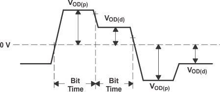
The high-speed data output driver consists of a voltage mode logic (VML) differential pair optimized for a 50-Ω impedance environment. The magnitude of the differential-pair signal swing is compatible with pseudo emitter coupled logic (PECL) levels when AC coupled. The line can be directly coupled or AC coupled. See Figure 6-7 and Figure 6-8 for termination details. The outputs also provide preemphasis to compensate for AC loss when driving a cable or PCB backplane trace over a long distance (see Figure 6-3). The level of preemphasis is controlled by PRE (see Table 6-2).
 Figure 6-3 Output Voltage Under Preemphasis (VTXP to VTXN)
Table 6-2 Programmable Preemphasis
| PRE | PREEMPHASIS LEVEL (%) VOD(P), VOD(D)(1) |
|---|---|
| 0 | 5% |
| 1 | 20% |
(1) VOD(p): Voltage swing when there is a transition in the data stream.
VOD(d): Voltage swing when there is no transition in the data stream.
VOD(d): Voltage swing when there is no transition in the data stream.