SLOSE29B November 2018 – August 2024 TLV1704-SEP
PRODUCTION DATA
- 1
- 1 Features
- 2 Applications
- 3 Description
- 4 Pin Configuration and Functions
- 5 Specifications
- 6 Detailed Description
- 7 Application and Implementation
- 8 Device and Documentation Support
- 9 Revision History
- 10Mechanical, Packaging, and Orderable Information
Package Options
Mechanical Data (Package|Pins)
- PW|14
Thermal pad, mechanical data (Package|Pins)
Orderable Information
3 Description
The TLV1704-SEP (Quad) device offers a wide supply range, rail-to-rail inputs, low quiescent current, and low propagation delay. All these features come in an industry-standard, TSSOP-14 plastic package, making these devices appropriate for applications where size, weight, and design flexibility are important..
The open-collector output offers the advantage of allowing the output to be level shifted to any voltage rail up to 24V above the negative power supply, regardless of the TLV1704-SEP supply voltage. Likewise, the outputs can be wired together to form a single alert signal.
The device is a microPower comparator. Low input offset voltage, low input bias currents, low supply current, and open-collector configuration make the TLV1704-SEP device well-suited for system diagnostics such as voltage monitoring, current sensing, and zero-cross detection.
| PART NUMBER | GRADE (1) | PACKAGE (2) |
|---|---|---|
| TLV1704AMPWTPSEP | 30krad(Si) RLAT | TSSOP (14) |
| TLV1704AMPWPSEP |
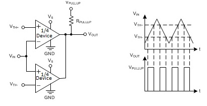
 TLV1704-SEP as a Window
Comparator
 Stable Propagation Delay vs
Temperature