SLOSE29B November 2018 – August 2024 TLV1704-SEP
PRODUCTION DATA
- 1
- 1 Features
- 2 Applications
- 3 Description
- 4 Pin Configuration and Functions
- 5 Specifications
- 6 Detailed Description
- 7 Application and Implementation
- 8 Device and Documentation Support
- 9 Revision History
- 10Mechanical, Packaging, and Orderable Information
Package Options
Mechanical Data (Package|Pins)
- PW|14
Thermal pad, mechanical data (Package|Pins)
Orderable Information
4 Pin Configuration and Functions
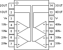
 Figure 4-1 TLV1704-SEP PW Package
14-Pin TSSOP
Top View
Table 4-1 Pin Functions
| PIN | I/O | DESCRIPTION | |||
|---|---|---|---|---|---|
| NAME | NO. | ||||
| IN+ | — | I | Noninverting input. | ||
| 1IN+ | 5 | I | Noninverting input, channel 1. | ||
| 2IN+ | 7 | I | Noninverting input, channel 2. | ||
| 3IN+ | 9 | I | Noninverting input, channel 3. | ||
| 4IN+ | 11 | I | Noninverting input, channel 4. | ||
| IN– | — | I | Inverting input. | ||
| 1IN– | 4 | I | Inverting input, channel 1. | ||
| 2IN– | 6 | I | Inverting input, channel 2. | ||
| 3IN– | 8 | I | Inverting input, channel 3. | ||
| 4IN– | 10 | I | Inverting input, channel 4. | ||
| OUT | — | O | Output. | ||
| 1OUT | 2 | O | Output, channel 1. | ||
| 2OUT | 1 | O | Output, channel 2. | ||
| 3OUT | 14 | O | Output, channel 3. | ||
| 4OUT | 13 | O | Output, channel 4. | ||
| V+ | 3 | — | Positive (highest) power supply. | ||
| V– | 12 | — | Negative (lowest) power supply. | ||