SBOS858 April 2017 TLV171-Q1
PRODUCTION DATA.
- 1 Features
- 2 Applications
- 3 Description
- 4 Description (continued)
- 5 Pin Configuration and Functions
- 6 Specifications
- 7 Detailed Description
- 8 Application and Implementation
- 9 Power Supply Recommendations
- 10Layout
- 11Device and Documentation Support
- 12Mechanical, Packaging, and Orderable Information
Package Options
Mechanical Data (Package|Pins)
- DBV|5
Thermal pad, mechanical data (Package|Pins)
Orderable Information
6 Specifications
6.1 Absolute Maximum Ratings
over operating free-air temperature range (unless otherwise noted)(1)| MIN | MAX | UNIT | ||
|---|---|---|---|---|
| Supply voltage, VS | 40 | V | ||
| Signal input terminals | Voltage | (V–) – 0.5 | (V+) + 0.5 | V |
| Current | ±10 | mA | ||
| Output short circuit(2) | Continuous | |||
| Junction temperature, TJ | 150 | °C | ||
| Latch-up per JESD78D | Class 1 | |||
| Storage temperature, Tstg | –65 | 150 | °C | |
(1) Stresses above these ratings may cause permanent damage. Exposure to absolute maximum conditions for extended periods may degrade device reliability. These are stress ratings only, and functional operation of the device at these or any other conditions beyond those specified is not implied.
(2) Short-circuit to ground, one amplifier per package.
6.2 ESD Ratings
| VALUE | UNIT | ||||
|---|---|---|---|---|---|
| TLV171-Q1 IN DBV PACKAGE | |||||
| V(ESD) | Electrostatic discharge | Human body model (HBM), per AEC Q100-002(1) | ±4000 | V | |
| Charged device model (CDM), per AEC Q100-011 | ±500 | ||||
| TLV2171-Q1 IN D AND DGK PACKAGES | |||||
| V(ESD) | Electrostatic discharge | Human body model (HBM), per AEC Q100-002(1) | ±4000 | V | |
| Charged device model (CDM), per AEC Q100-011 | ±1000 | ||||
| TLV4171-Q1 IN D AND PW PACKAGES | |||||
| V(ESD) | Electrostatic discharge | Human body model (HBM), per AEC Q100-002(1) | ±2000 | V | |
| Charged device model (CDM), per AEC Q100-011 | ±1000 | ||||
(1) AEC Q100-002 indicates HBM stressing is done in accordance with the ANSI/ESDA/JEDEC JS-001 specification.
6.3 Recommended Operating Conditions
over operating free-air temperature range (unless otherwise noted)| MIN | NOM | MAX | UNIT | ||
|---|---|---|---|---|---|
| Supply voltage (V+ – V–) | 4.5 (±2.25) | 36 (±18) | V | ||
| Specified operating temperature | –40 | 125 | °C | ||
6.4 Thermal Information: TLV171-Q1
| THERMAL METRIC(1) | TLV171-Q1 | UNIT | |
|---|---|---|---|
| DBV (SOT-23) | |||
| 5 PINS | |||
| RθJA | Junction-to-ambient thermal resistance | 277.3 | °C/W |
| RθJC(top) | Junction-to-case (top) thermal resistance | 193.3 | °C/W |
| RθJB | Junction-to-board thermal resistance | 121.2 | °C/W |
| ψJT | Junction-to-top characterization parameter | 51.8 | °C/W |
| ψJB | Junction-to-board characterization parameter | 109.5 | °C/W |
(1) For more information about traditional and new thermal metrics, see the Semiconductor and IC Package Thermal Metrics application report.
6.5 Thermal Information: TLV2171-Q1
| THERMAL METRIC(1) | TLV2171-Q1 | UNIT | ||
|---|---|---|---|---|
| D (SOIC) | DGK (VSSOP) | |||
| 8 PINS | 8 PINS | |||
| RθJA | Junction-to-ambient thermal resistance | 116.1 | 186.5 | °C/W |
| RθJC(top) | Junction-to-case (top) thermal resistance | 69.8 | 78 | °C/W |
| RθJB | Junction-to-board thermal resistance | 56.6 | 107.8 | °C/W |
| ψJT | Junction-to-top characterization parameter | 22.5 | 15.6 | °C/W |
| ψJB | Junction-to-board characterization parameter | 56.1 | 106.2 | °C/W |
(1) For more information about traditional and new thermal metrics, see the Semiconductor and IC Package Thermal Metrics application report.
6.6 Thermal Information: TLV4171-Q1
| THERMAL METRIC(1) | TLV4171-Q1 | UNIT | ||
|---|---|---|---|---|
| D (SOIC) | PW (TSSOP) | |||
| 14 PINS | 14 PINS | |||
| RθJA | Junction-to-ambient thermal resistance | 93.2 | 106.9 | °C/W |
| RθJC(top) | Junction-to-case (top) thermal resistance | 51.8 | 24.4 | °C/W |
| RθJB | Junction-to-board thermal resistance | 49.4 | 59.3 | °C/W |
| ψJT | Junction-to-top characterization parameter | 13.5 | 0.6 | °C/W |
| ψJB | Junction-to-board characterization parameter | 42.2 | 54.3 | °C/W |
(1) For more information about traditional and new thermal metrics, see the Semiconductor and IC Package Thermal Metrics application report.
6.7 Electrical Characteristics
at TA = 25°C, VS = 4.5 V to 36 V, VCM = VOUT = VS / 2, and RLOAD = 10 kΩ connected to VS / 2 (unless otherwise noted)| PARAMETER | TEST CONDITIONS | MIN | TYP | MAX | UNIT | |
|---|---|---|---|---|---|---|
| OFFSET VOLTAGE | ||||||
| VOS | Input offset voltage | 0.75 | ±2.7 | mV | ||
| Input offset voltage over temperature | TA = –40°C to 125°C | ±3 | mV | |||
| dVOS/dT | Input offset voltage drift (over temperature) |
TA = –40°C to 125°C |
1 |
µV/°C | ||
| PSRR | Input offset voltage over temperature vs power supply | VS = 4.5 V to 36 V | 90 | 120 | dB | |
| INPUT BIAS CURRENT | ||||||
| IB | Input bias current |
±10 |
pA | |||
| IOS | Input offset current | ±4 | pA | |||
| NOISE | ||||||
| Input voltage noise | f = 0.1 Hz to 10 Hz | 3 | µVPP | |||
| en | Input voltage noise density | f = 100 Hz | 27 | nV/√Hz | ||
| f = 1 kHz | 16 | nV/√Hz | ||||
| INPUT VOLTAGE | ||||||
| VCM | Common-mode voltage range(1) | (V–) – 0.1 | (V+) – 2 | V | ||
| CMRR | Common-mode rejection ratio (over temperature) | VS = ±2.25 V (V–) – 0.1 V < VCM < (V+) – 2 V |
90 |
120 |
dB | |
| VS = ±18 V (V–) – 0.1 V < VCM < (V+) – 2 V |
94 |
120 |
dB | |||
| INPUT IMPEDANCE | ||||||
| Differential | 100 || 3 | MΩ || pF | ||||
| Common-mode | 6 || 3 | 1012Ω || pF | ||||
| OPEN-LOOP GAIN | ||||||
| AOL | Open-loop voltage gain (over temperature) | VS = 4.5 V to 36 V (V–) + 0.35 V < VO < (V+) – 0.35 V |
94 |
130 | dB | |
| FREQUENCY RESPONSE | ||||||
| GBP | Gain bandwidth product | 3 | MHz | |||
| SR | Slew rate | G = 1 | 1.5 | V/µs | ||
| tS | Settling time | To 0.1%, VS = ±18 V G = 1, 10-V step |
6 | µs | ||
| To 0.01% (12 bit), VS = ±18 V G = 1, 10-V step |
10 | µs | ||||
| Overload recovery time | V±IN × Gain > VS | 2 | µs | |||
| THD+N | Total harmonic distortion + noise | G = 1, f = 1 kHz VO = 3 VRMS |
0.0002% | |||
| OUTPUT | ||||||
| VO | Voltage output swing from rail (over temperature) | RL = 10 kΩ AOL ≥ 110 dB |
(V–) + 0.35 | (V+) – 0.35 | V | |
| ISC | Short-circuit current | Sourcing | 25 | mA | ||
| Sinking | –37 | |||||
| CLOAD | Capacitive load drive | See Typical Characteristics | pF | |||
| RO | Open-loop output resistance | f = 1 MHz, IO = 0 A | 150 | Ω | ||
| POWER SUPPLY | ||||||
| VS | Specified voltage range | TA = –40°C to 125°C | 4.5 | 36 | V | |
| IQ | Quiescent current per amplifier | IO = 0 A, TA = –40°C to 125°C | 525 |
695 |
µA | |
(1) The input range can be extended beyond (V+) – 2 V up to V+ at reduced performance. See Typical Characteristics and Detailed Description for additional information.
6.8 Typical Characteristics
VS = ±18 V, VCM = VS / 2, RLOAD = 10 kΩ connected to VS / 2, and CL = 100 pF (unless otherwise noted)Table 2. Characteristic Performance Measurements
| DESCRIPTION | FIGURE |
|---|---|
| Offset Voltage Production Distribution | Figure 1 |
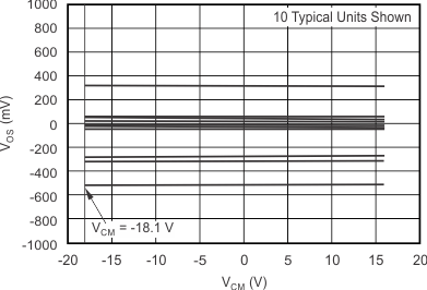
| Offset Voltage vs Common-Mode Voltage | Figure 2 |
| Offset Voltage vs Common-Mode Voltage (Upper Stage) | Figure 3 |
| Input Bias Current vs Temperature | Figure 5 |
| Output Voltage Swing vs Output Current (Maximum Supply) | Figure 6 |
| CMRR and PSRR vs Frequency (Referred-to Input) | Figure 7 |
| 0.1Hz to 10Hz Noise | Figure 8 |
| Input Voltage Noise Spectral Density vs Frequency | Figure 9 |
| Quiescent Current vs Supply Voltage | Figure 10 |
| Open-Loop Gain and Phase vs Frequency | Figure 11 |
| Closed-Loop Gain vs Frequency | Figure 12 |
| Open-Loop Gain vs Temperature | Figure 13 |
| Open-Loop Output Impedance vs Frequency | Figure 14 |
| Small-Signal Overshoot vs Capacitive Load (100-mV Output Step) | Figure 15, |
| No Phase Reversal | Figure 17 |
| Small-Signal Step Response (100 mV) | Figure 18, Figure 19 |
| Large-Signal Step Response | Figure 20, Figure 21 |
| Large-Signal Settling Time (10-V Positive Step) | Figure 22 |
| Large-Signal Settling Time (10-V Negative Step) | Figure 23 |
| Short-Circuit Current vs Temperature | Figure 24 |
| Maximum Output Voltage vs Frequency | Figure 25 |
6.8.1 Typical Characteristics


(Upper Stage)


(Referred-to Input)


| RL = 10 kΩ |
(100-mV Output Step)


| CL = 100 pF |

| G = –1 | RL = 10 kΩ | CL = 100 pF |

| G = –1 |


(100-mV Output Step)

| RL = 10 kΩ | CL = 100 pF |

| G = 1 | RL = 10 kΩ | CL = 100 pF |

| G = –1 |
