SNOSDC8D September   2022  – December 2024 TLV1811 , TLV1812 , TLV1814 , TLV1821 , TLV1822 , TLV1824

PRODMIX  

  1.   1
  2. Features
  3. Applications
  4. Description
  5. Pin Configuration and Functions
    1.     Pin Functions: TLV18x1 and TLV18x1L
    2.     Pin Functions: TLV1812 and TLV1822
    3.     Pin Functions: TLV1814 and TLV1824
  6. Specifications
    1. 5.1 Absolute Maximum Ratings
    2. 5.2 ESD Ratings
    3. 5.3 Recommended Operating Conditions
    4. 5.4 Thermal Information - Single
    5. 5.5 Thermal Information - EP
    6. 5.6 Thermal Information - Quad
    7. 5.7 Electrical Characteristics
    8. 5.8 Switching Characteristics
  7. Typical Characteristics
  8. Detailed Description
    1. 7.1 Overview
    2. 7.2 Functional Block Diagrams
    3. 7.3 Feature Description
    4. 7.4 Device Functional Modes
      1. 7.4.1 Inputs
        1. 7.4.1.1 TLV18xx Rail-to-Rail Input
        2. 7.4.1.2 ESD Protection
        3. 7.4.1.3 Unused Inputs
      2. 7.4.2 Outputs
        1. 7.4.2.1 TLV181x Push-Pull Output
        2. 7.4.2.2 TLV182x Open-Drain Output
      3. 7.4.3 Power-On Reset (POR)
      4. 7.4.4 Hysteresis
  9. Application and Implementation
    1. 8.1 Application Information
      1. 8.1.1 Basic Comparator Definitions
        1. 8.1.1.1 Operation
        2. 8.1.1.2 Propagation Delay
        3. 8.1.1.3 Overdrive and Underdrive Voltage
      2. 8.1.2 Hysteresis
        1. 8.1.2.1 Inverting Comparator With Hysteresis
        2. 8.1.2.2 Non-Inverting Comparator With Hysteresis
        3. 8.1.2.3 Inverting and Non-Inverting Hysteresis using Open-Drain Output
    2. 8.2 Typical Applications
      1. 8.2.1 Window Comparator
        1. 8.2.1.1 Design Requirements
        2. 8.2.1.2 Detailed Design Procedure
        3. 8.2.1.3 Application Curve
      2. 8.2.2 Square-Wave Oscillator
        1. 8.2.2.1 Design Requirements
        2. 8.2.2.2 Detailed Design Procedure
        3. 8.2.2.3 Application Curve
      3. 8.2.3 Adjustable Pulse Width Generator
      4. 8.2.4 Time Delay Generator
      5. 8.2.5 Logic Level Shifter
      6. 8.2.6 One-Shot Multivibrator
      7. 8.2.7 Bi-Stable Multivibrator
      8. 8.2.8 Zero Crossing Detector
      9. 8.2.9 Pulse Slicer
    3. 8.3 Power Supply Recommendations
    4. 8.4 Layout
      1. 8.4.1 Layout Guidelines
      2. 8.4.2 Layout Example
  10. Device and Documentation Support
    1. 9.1 Documentation Support
      1. 9.1.1 Related Documentation
    2. 9.2 Receiving Notification of Documentation Updates
    3. 9.3 Support Resources
    4. 9.4 Trademarks
    5. 9.5 Electrostatic Discharge Caution
    6. 9.6 Glossary
  11. 10Revision History
  12. 11Mechanical, Packaging, and Orderable Information

Package Options

Mechanical Data (Package|Pins)
Thermal pad, mechanical data (Package|Pins)
Orderable Information

Logic Level Shifter

The output of the TLV182x is the uncommitted drain of the output transistor. Many open-drain outputs can be tied together to provide an output OR'ing function if desired.
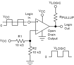
TLV1811 TLV1821 TLV1812 TLV1822 TLV1814 TLV1824 Universal Logic Level ShifterFigure 8-14 Universal Logic Level Shifter

The two 10kΩ resistors bias the input to half of the input logic supply level to set the threshold in the mid-point of the input logic levels. Only one shared output pull-up resistor is needed and can be connected to any pull-up voltage between 0V and 5.5V. The pullup voltage (VLOGIC) must match the driven logic input "high" level.