SNOSDC9C October   2022  – December 2024 TLV1811-Q1 , TLV1812-Q1 , TLV1814-Q1 , TLV1821-Q1 , TLV1822-Q1 , TLV1824-Q1

PRODMIX  

  1.   1
  2. Features
  3. Applications
  4. Description
  5. Pin Configuration and Functions
    1.     Pin Functions: TLV18x1-Q1 and TLV18x1L-Q1
    2.     Pin Functions: TLV1812-Q1 and TLV1822-Q1
    3.     Pin Functions: TLV1814-Q1 and TLV1824-Q1
  6. Specifications
    1. 5.1 Absolute Maximum Ratings
    2. 5.2 ESD Ratings
    3. 5.3 Recommended Operating Conditions
    4. 5.4 Thermal Information - Single
    5. 5.5 Thermal Information - EP
    6. 5.6 Thermal Information - Quad
    7. 5.7 Electrical Characteristics
    8. 5.8 Switching Characteristics
  7. Typical Characteristics
  8. Detailed Description
    1. 7.1 Overview
    2. 7.2 Functional Block Diagrams
    3. 7.3 Feature Description
    4. 7.4 Device Functional Modes
      1. 7.4.1 Inputs
        1. 7.4.1.1 TLV18xx Rail-to-Rail Input
        2. 7.4.1.2 ESD Protection
        3. 7.4.1.3 Unused Inputs
      2. 7.4.2 Outputs
        1. 7.4.2.1 TLV181x-Q1 Push-Pull Output
        2. 7.4.2.2 TLV182x-Q1 Open-Drain Output
      3. 7.4.3 Power-On Reset (POR)
      4. 7.4.4 Hysteresis
  9. Application and Implementation
    1. 8.1 Application Information
      1. 8.1.1 Basic Comparator Definitions
        1. 8.1.1.1 Operation
        2. 8.1.1.2 Propagation Delay
        3. 8.1.1.3 Overdrive and Underdrive Voltage
      2. 8.1.2 Hysteresis
        1. 8.1.2.1 Inverting Comparator With Hysteresis
        2. 8.1.2.2 Non-Inverting Comparator With Hysteresis
        3. 8.1.2.3 Inverting and Non-Inverting Hysteresis using Open-Drain Output
    2. 8.2 Typical Applications
      1. 8.2.1 Window Comparator
        1. 8.2.1.1 Design Requirements
        2. 8.2.1.2 Detailed Design Procedure
        3. 8.2.1.3 Application Curve
      2. 8.2.2 Square-Wave Oscillator
        1. 8.2.2.1 Design Requirements
        2. 8.2.2.2 Detailed Design Procedure
        3. 8.2.2.3 Application Curve
      3. 8.2.3 Adjustable Pulse Width Generator
      4. 8.2.4 Time Delay Generator
      5. 8.2.5 Logic Level Shifter
      6. 8.2.6 One-Shot Multivibrator
      7. 8.2.7 Bi-Stable Multivibrator
      8. 8.2.8 Zero Crossing Detector
      9. 8.2.9 Pulse Slicer
    3. 8.3 Power Supply Recommendations
    4. 8.4 Layout
      1. 8.4.1 Layout Guidelines
      2. 8.4.2 Layout Example
  10. Device and Documentation Support
    1. 9.1 Documentation Support
      1. 9.1.1 Related Documentation
    2. 9.2 Receiving Notification of Documentation Updates
    3. 9.3 Support Resources
    4. 9.4 Trademarks
    5. 9.5 Electrostatic Discharge Caution
    6. 9.6 Glossary
  11. 10Revision History
  12. 11Mechanical, Packaging, and Orderable Information

Package Options

Mechanical Data (Package|Pins)
Thermal pad, mechanical data (Package|Pins)
Orderable Information

Zero Crossing Detector

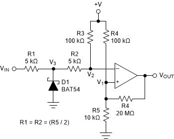
TLV1811-Q1 TLV1821-Q1 TLV1812-Q1 TLV1822-Q1  TLV1814-Q1 TLV1824-Q1 Zero Crossing DetectorFigure 8-17 Zero Crossing Detector

A voltage divider of R4 and R5 establishes a reference voltage V1 at the non-inverting input. By making the series resistance of R1 and R2 equal to R5, the comparator output switches when VIN = 0V. Diode D1 clamps V3 near ground. The voltage divider of R2 and R3 then prevents V2 from going below ground. A small amount of hysteresis is setup to maintain rapid output voltage transitions.