SNOSDG6 September   2024 TLV1831-Q1

ADVANCE INFORMATION  

  1.   1
  2. Features
  3. Applications
  4. Description
  5. Pin Configuration and Functions
    1.     Pin Configuration: TLV1831-Q1 and TLV1841-Q1
    2.     Pin Configurations: TLV1832-Q1 and TLV1842-Q1
    3.     Pin Configuration and Functions: TLV1834-Q1 and TLV1844-Q1
  6. Specifications
    1. 5.1 Absolute Maximum Ratings
    2. 5.2 ESD Ratings
    3. 5.3 Thermal Information
    4. 5.4 Recommended Operating Conditions
    5. 5.5 Electrical Characteristics
    6. 5.6 Switching Characteristics
    7. 5.7 Typical Characteristics
  7. Detailed Description
    1. 6.1 Overview
    2. 6.2 Functional Block Diagrams
    3. 6.3 Feature Description
    4. 6.4 Device Functional Modes
      1. 6.4.1 Inputs
        1. 6.4.1.1 Rail-to-Rail Input
        2. 6.4.1.2 Unused Inputs
      2. 6.4.2 Outputs
        1. 6.4.2.1 TLV183x-Q1 Push-Pull Output
        2. 6.4.2.2 TLV184x-Q1 Open-Drain Output
      3. 6.4.3 ESD Protection
        1. 6.4.3.1 Inputs
        2. 6.4.3.2 Outputs
      4. 6.4.4 Power-On Reset (POR)
  8. Application and Implementation
    1. 7.1 Application Information
      1. 7.1.1 Basic Comparator Definitions
        1. 7.1.1.1 Operation
        2. 7.1.1.2 Propagation Delay
        3. 7.1.1.3 Overdrive Voltage
      2. 7.1.2 Hysteresis
        1. 7.1.2.1 Inverting Comparator With Hysteresis
        2. 7.1.2.2 Non-Inverting Comparator With Hysteresis
        3. 7.1.2.3 Inverting and Non-Inverting Hysteresis using Open-Drain Output
    2. 7.2 Typical Applications
      1. 7.2.1 Window Comparator
        1. 7.2.1.1 Design Requirements
        2. 7.2.1.2 Detailed Design Procedure
        3. 7.2.1.3 Application Curve
      2. 7.2.2 Square Wave Oscillator
        1. 7.2.2.1 Design Requirements
        2. 7.2.2.2 Detailed Design Procedure
        3. 7.2.2.3 Application Performance Plots
    3. 7.3 Power Supply Recommendations
    4. 7.4 Layout
      1. 7.4.1 Layout Guidelines
      2. 7.4.2 Layout Example
  9. Device and Documentation Support
    1. 8.1 Documentation Support
      1. 8.1.1 Related Documentation
    2. 8.2 Receiving Notification of Documentation Updates
    3. 8.3 Support Resources
    4. 8.4 Trademarks
    5. 8.5 Electrostatic Discharge Caution
    6. 8.6 Glossary
  10. Revision History
  11. 10Mechanical, Packaging, and Orderable Information

Package Options

Mechanical Data (Package|Pins)
Thermal pad, mechanical data (Package|Pins)
Orderable Information

Description

The TLV183x-Q1 and TLV184x-Q1 are high-speed comparators with operating voltages up to 40V. The comparators offer rail-to-rail inputs with push-pull and open-drain output options. These features coupled with 65ns propagation delay make this family well-suited for high speed current sensing and voltage protection applications.

All devices include a Power-On Reset (POR) feature that makes sure the output is in a known state until the minimum supply voltage has been reached. Once this voltage has been reached, the output responds to the inputs, thus preventing false outputs during system power-up and power-down.

The TLV183x-Q1 comparators have a push-pull output stage, which are designed for applications where symmetry between rising and falling output responses is desired. The TLV184x-Q1 comparators have an open-drain output stage, making them appropriate for level transition.

Device Information
PART NUMBERPACKAGE (1)BODY SIZE (NOM)(2)
TLV1831-Q1, TLV1841-Q1SC-70 (5)2.00mm × 2.00mm
TLV1832-Q1, TLV1842-Q1VSSOP (8)3.00mm × 3.00mm
TSSOP (8)3.00mm × 4.40mm
WSON (8) (Preview)2.00mm × 2.00mm
TLV1834-Q1, TLV1844-Q1SOT-23 (14) (Preview)4.20mm × 2.00mm
WQFN (16) (Preview)3.00mm × 3.00mm
For all available packages, see the orderable addendum at the end of the data sheet.
The package size (length × width) is a nominal value and includes pins, where applicable.
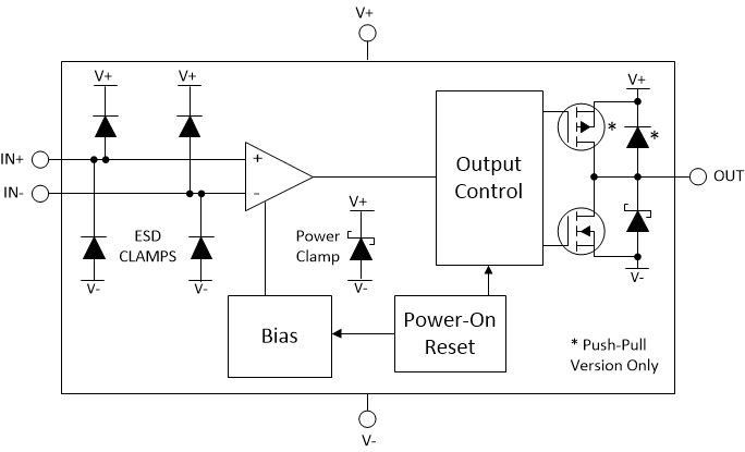
TLV1831-Q1 TLV1841-Q1 TLV1832-Q1 TLV1842-Q1  Functional Block DiagramFunctional Block Diagram
TLV1831-Q1 TLV1841-Q1 TLV1832-Q1 TLV1842-Q1  Propagation
                        Delay, (Low to High) vs. Input Overdrive, 12VPropagation Delay, (Low to High) vs. Input Overdrive, 12V