SNOSDE7B December   2022  – September 2024 TLV1851 , TLV1852 , TLV1854 , TLV1861 , TLV1862 , TLV1864

PRODMIX  

  1.   1
  2. Features
  3. Applications
  4. Description
  5. Pin Configuration and Functions
    1.     Pin Configuration: TLV1831 and TLV1841
    2.     Pin Configurations: TLV1852 and TLV1862
    3.     Pin Configurations: TLV1854 and TLV1864
  6. Specifications
    1. 5.1 Absolute Maximum Ratings
    2. 5.2 ESD Ratings
    3. 5.3 Thermal Information
    4. 5.4 Recommended Operating Conditions
    5. 5.5 Electrical Characteristics
    6. 5.6 Switching Characteristics
    7. 5.7 Typical Characteristics
  7. Detailed Description
    1. 6.1 Overview
    2. 6.2 Functional Block Diagrams
    3. 6.3 Feature Description
    4. 6.4 Device Functional Modes
      1. 6.4.1 Inputs
        1. 6.4.1.1 Operating Common-Mode Ranges
        2. 6.4.1.2 Fail-Safe Inputs
        3. 6.4.1.3 Unused Inputs
      2. 6.4.2 Internal Hysteresis
      3. 6.4.3 Outputs
        1. 6.4.3.1 TLV185x Push-Pull Output
        2. 6.4.3.2 TLV186x Open-Drain Output
      4. 6.4.4 ESD Protection
        1. 6.4.4.1 Inputs
        2. 6.4.4.2 Outputs
      5. 6.4.5 Power-On Reset (POR)
      6. 6.4.6 Reverse Battery Protection
  8. Application and Implementation
    1. 7.1 Application Information
      1. 7.1.1 Basic Comparator Definitions
        1. 7.1.1.1 Operation
        2. 7.1.1.2 Propagation Delay
        3. 7.1.1.3 Overdrive Voltage
      2. 7.1.2 Hysteresis
        1. 7.1.2.1 Inverting Comparator With Hysteresis
        2. 7.1.2.2 Non-Inverting Comparator With Hysteresis
        3. 7.1.2.3 Inverting and Non-Inverting Hysteresis using Open-Drain Output
    2. 7.2 Typical Applications
      1. 7.2.1 Window Comparator
        1. 7.2.1.1 Design Requirements
        2. 7.2.1.2 Detailed Design Procedure
        3. 7.2.1.3 Application Curve
      2. 7.2.2 Undervoltage Detection
      3. 7.2.3 Reverse Battery and Overvoltage Protection Scheme
    3. 7.3 Power Supply Recommendations
    4. 7.4 Layout
      1. 7.4.1 Layout Guidelines
      2. 7.4.2 Layout Example
  9. Device and Documentation Support
    1. 8.1 Documentation Support
      1. 8.1.1 Related Documentation
    2. 8.2 Receiving Notification of Documentation Updates
    3. 8.3 Support Resources
    4. 8.4 Trademarks
    5. 8.5 Electrostatic Discharge Caution
    6. 8.6 Glossary
  10. Revision History
  11. 10Mechanical, Packaging, and Orderable Information

Package Options

Mechanical Data (Package|Pins)
Thermal pad, mechanical data (Package|Pins)
Orderable Information

Propagation Delay

There is a delay between from when the input crosses the reference voltage and the output responds. This is called the Propagation Delay. Propagation delay can be different between high-to low and low-to-high input transitions. This is shown as tpLH and tpHL in Figure 7-1 and is measured from the mid-point of the input to the midpoint of the output.
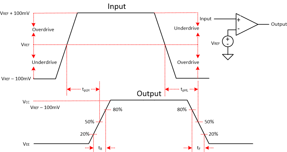
TLV1851 TLV1861 TLV1852 TLV1862 TLV1854 TLV1864 Comparator Timing DiagramFigure 7-1 Comparator Timing Diagram