SBOS935B April   2020  – July 2020 TLV197-Q1 , TLV2197-Q1 , TLV4197-Q1

PRODUCTION DATA.  

  1. Features
  2. Applications
  3. Description
    1.     Device Images
      1.      TLVx197-Q1 Detect Voltages in Automotive Applications
  4. Revision History
  5. Pin Configuration and Functions
    1.     Pin Functions: TLV197-Q1
    2.     Pin Functions: TLV2197-Q1
    3.     Pin Functions: TLV4197-Q1
  6. Specifications
    1. 6.1 Absolute Maximum Ratings
    2. 6.2 ESD Ratings
    3. 6.3 Recommended Operating Conditions
    4. 6.4 Thermal Information: TLV197-Q1
    5. 6.5 Thermal Information: TLV2197-Q1
    6. 6.6 Thermal Information: TLV4197-Q1
    7. 6.7 Electrical Characteristics: VS = ±4 V to ±18 V (VS = 8 V to 36 V)
    8. 6.8 Electrical Characteristics: VS = ±2.25 V to ±4 V (VS = 4.5 V to 8 V)
    9. 6.9 Typical Characteristics
  7. Detailed Description
    1. 7.1 Overview
    2. 7.2 Functional Block Diagram
    3. 7.3 Feature Description
      1. 7.3.1 Input Protection Circuitry
      2. 7.3.2 EMI Rejection
      3. 7.3.3 Phase Reversal Protection
      4. 7.3.4 Thermal Protection
      5. 7.3.5 Capacitive Load and Stability
      6. 7.3.6 Common-Mode Voltage Range
      7. 7.3.7 Electrical Overstress
      8. 7.3.8 Overload Recovery
    4. 7.4 Device Functional Modes
  8. Application and Implementation
    1. 8.1 Application Information
    2. 8.2 Typical Applications
      1. 8.2.1 16-Bit Precision Multiplexed Data-Acquisition System
        1. 8.2.1.1 Design Requirements
        2. 8.2.1.2 Detailed Design Procedure
        3. 8.2.1.3 Application Curve
      2. 8.2.2 Slew-Rate Limit for Input Protection
      3. 8.2.3 Precision Reference Buffer
  9. Power Supply Recommendations
  10. 10Layout
    1. 10.1 Layout Guidelines
    2. 10.2 Layout Examples
  11. 11Device and Documentation Support
    1. 11.1 Device Support
      1. 11.1.1 Development Support
        1. 11.1.1.1 TINA-TI (Free Software Download)
    2. 11.2 Documentation Support
      1. 11.2.1 Related Documentation
    3. 11.3 Related Links
    4. 11.4 Receiving Notification of Documentation Updates
    5. 11.5 Support Resources
    6. 11.6 Trademarks
    7. 11.7 Electrostatic Discharge Caution
    8. 11.8 Glossary
  12. 12Mechanical, Packaging, and Orderable Information

Package Options

Mechanical Data (Package|Pins)
Thermal pad, mechanical data (Package|Pins)
Orderable Information

Application Curve

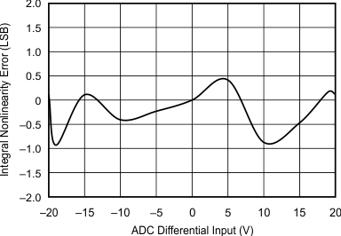
TLV197-Q1 TLV2197-Q1 TLV4197-Q1 ai_linearity_error_bos620.gifFigure 42. ADC 16-Bit Linearity Error for the Multiplexed Data Acquisition Block
For step-by-step design procedure, circuit schematics, bill of materials, PCB files, simulation results, and test results, refer to TIPD151, 16-Bit, 400 kSPS 4-Channell, Multiplexed Data Acquisition Ref erence Design for High Voltage Inputs, Low Distortion.