SLVS067M March 1992 – November 2016 TLV2217
PRODUCTION DATA.
- 1 Features
- 2 Applications
- 3 Description
- 4 Revision History
- 5 Pin Configuration and Functions
- 6 Specifications
- 7 Detailed Description
- 8 Application and Implementation
- 9 Power Supply Recommendations
- 10Layout
- 11Device and Documentation Support
- 12Mechanical, Packaging, and Orderable Information
Package Options
Refer to the PDF data sheet for device specific package drawings
Mechanical Data (Package|Pins)
- KVU|3
- KCS|3
- PW|20
Thermal pad, mechanical data (Package|Pins)
- KVU|3
Orderable Information
7 Detailed Description
7.1 Overview
The TLV2217 device is a positive low-dropout voltage regulator designed to provide up to 500 mA of output current. The device is available in 1.8-V, 2.5-V, and 3.3-V options. All internal circuitry is designed to operate down to 0.5-V input-to-output differential, with the minimum input voltage of 3 V for all voltage options.
The TLV2217 device is designed to be stable with tantalum and aluminum electrolytic output capacitors having an ESR between 0.4 Ω and 2 Ω.
The TLV2217 device is characterized for operation over the virtual junction temperature range of 0°C to 125°C.
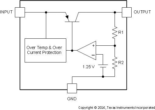
7.2 Functional Block Diagram

7.3 Feature Description
7.3.1 Overload Block
Current limiting and overtemperature shutdown protects against overload by turning off the PNP pass element.
7.4 Device Functional Modes
7.4.1 Operation With Low Input Voltage
The TLV2217 device requires 0.5-V headroom (VI – VO) to operate in regulation. With less headroom, the device may drop out and OUTPUT voltage is INPUT voltage minus dropout voltage.
7.4.2 Operation at Light Loads
The load or feedback must consume the minimum bias current defined in Electrical Characteristics: TLV2217-33 for regulation, or the output may be too high.
7.4.3 Operation in Self Protection
When an overload occurs, the device shuts down the output stage or reduce the output current to prevent device damage. The device automatically resets from the overload. The output may be reduced or alternate between on and off until the overload is removed.