SLVS067M March 1992 – November 2016 TLV2217
PRODUCTION DATA.
- 1 Features
- 2 Applications
- 3 Description
- 4 Revision History
- 5 Pin Configuration and Functions
- 6 Specifications
- 7 Detailed Description
- 8 Application and Implementation
- 9 Power Supply Recommendations
- 10Layout
- 11Device and Documentation Support
- 12Mechanical, Packaging, and Orderable Information
Package Options
Refer to the PDF data sheet for device specific package drawings
Mechanical Data (Package|Pins)
- KVU|3
- KCS|3
- PW|20
Thermal pad, mechanical data (Package|Pins)
- KVU|3
Orderable Information
5 Pin Configuration and Functions
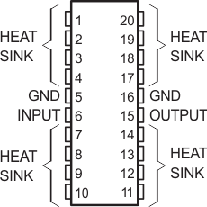
PW Package
20-Pin TSSOP
Top View

KVU Package
3-Pin TO-252
Top View

KCS Package
3-Pin TO-220
Top View

Pin Functions
| PIN | I/O | DESCRIPTION | |||
|---|---|---|---|---|---|
| NAME | PW | KVU | KCS | ||
| INPUT | 6 | 1 | 1 | I | Voltage input |
| OUTPUT | 15 | 3 | 3 | O | Voltage output |
| GND | 5, 16 | 2 | 2 | — | Ground |
| HEAT SINK | 1, 2, 3, 4, 7, 8, 9, 10, 11, 12, 13, 14 17, 18, 19, 20 |
— | — | — | Connection for improved thermal dissipation. These terminals have an internal resistive connection to ground and must be grounded or electrically isolated. |