SBOSAB8B June   2023  – September 2024 TLV2365-Q1 , TLV365-Q1

PRODMIX  

  1.   1
  2. Features
  3. Applications
  4. Description
  5. Device Comparison Table
  6. Pin Configuration and Functions
  7. Specifications
    1. 6.1 Absolute Maximum Ratings
    2. 6.2 ESD Ratings
    3. 6.3 Recommended Operating Conditions
    4. 6.4 Thermal Information
    5. 6.5 Electrical Characteristics
    6. 6.6 Typical Characteristics
  8. Detailed Description
    1. 7.1 Overview
    2. 7.2 Functional Block Diagram
    3. 7.3 Feature Description
      1. 7.3.1 Rail-to-Rail Input
      2. 7.3.2 Input and ESD Protection
      3. 7.3.3 Driving Capacitive Loads
      4. 7.3.4 Active Filter
    4. 7.4 Device Functional Modes
  9. Application and Implementation
    1. 8.1 Application Information
      1. 8.1.1 Overdrive Recovery Performance
      2. 8.1.2 Achieving an Output Level of Zero Volts
    2. 8.2 Typical Applications
      1. 8.2.1 Second-Order Low-Pass Filter
        1. 8.2.1.1 Design Requirements
        2. 8.2.1.2 Detailed Design Procedure
        3. 8.2.1.3 Application Curve
      2. 8.2.2 ADC Driver and Reference Buffer
    3. 8.3 Power Supply Recommendations
    4. 8.4 Layout
      1. 8.4.1 Layout Guidelines
      2. 8.4.2 Layout Example
  10. Device and Documentation Support
    1. 9.1 Device Support
      1. 9.1.1 Development Support
        1. 9.1.1.1 PSpice® for TI
        2. 9.1.1.2 TINA-TI™ Simulation Software (Free Download)
        3. 9.1.1.3 DIP-Adapter-EVM
        4. 9.1.1.4 DIYAMP-EVM
        5. 9.1.1.5 TI Reference Designs
        6. 9.1.1.6 Analog Filter Designer
    2. 9.2 Documentation Support
      1. 9.2.1 Related Documentation
    3. 9.3 Receiving Notification of Documentation Updates
    4. 9.4 Support Resources
    5. 9.5 Trademarks
    6. 9.6 Electrostatic Discharge Caution
    7. 9.7 Glossary
  11. 10Revision History
  12. 11Mechanical, Packaging, and Orderable Information

Package Options

Refer to the PDF data sheet for device specific package drawings

Mechanical Data (Package|Pins)
  • D|8
Thermal pad, mechanical data (Package|Pins)
Orderable Information

Input and ESD Protection

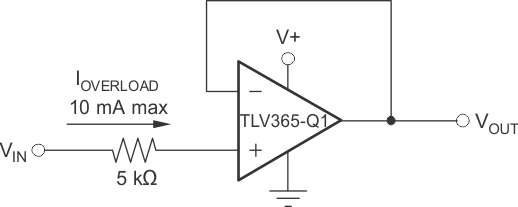
Figure 7-2 shows that the TLVx365-Q1 incorporates internal electrostatic discharge (ESD) protection circuits on all pins. In the case of input and output pins, this protection primarily consists of current-steering diodes connected between the input and power-supply pins. These ESD protection diodes also provide in-circuit, input overdrive protection if the current is limited to 10 mA; see also Section 6.1. Figure 7-3 shows how a series input resistor can be added to the driven input to limit the input current. The added resistor contributes thermal noise at the amplifier input; the resistor must be kept to the minimum value in noise-sensitive applications.

TLV365-Q1 TLV2365-Q1 ESD Protection
            SchemeFigure 7-2 ESD Protection Scheme
TLV365-Q1 TLV2365-Q1 Input Current
            ProtectionFigure 7-3 Input Current Protection