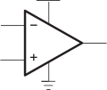
The TLV237x single-supply operational amplifiers provide rail-to-rail input and output capability. The TLV237x takes the minimum operating supply voltage down to 2.7 V over the extended industrial temperature range while adding the rail-to-rail output swing feature. The TLV237x also provides 3-MHz bandwidth from only 550 μA. The maximum recommended supply voltage is 16 V, which allows the devices to be operated from (±8-V supplies down to ±1.35 V) a variety of rechargeable cells.
The CMOS inputs enable use in high-impedance sensor interfaces, with the lower voltage operation making an ideal alternative for the TLC227x in battery-powered applications. The rail-to-rail input stage further increases its versatility. The TLV237x is the seventh member of a rapidly growing number of RRIO products available from TI, and it is the first to allow operation up to 16-V rails with good ac performance.
All members are available in PDIP and SOIC with the singles in the small SOT-23 package, duals in the MSOP, and quads in the TSSOP package.
The 2.7-V operation makes the TLV237x compatible with Li-Ion powered systems and the operating supply voltage range of many micro-power microcontrollers available today including TI’s MSP430.
PART NUMBER | PACKAGE | BODY SIZE (NOM) |
---|---|---|
TLV237x | PDIP (8) | 9.81 mm × 6.35 mm |
PDIP (14) | 19.30 mm × 6.35 mm | |
SOIC (8) | 4.90 mm × 3.91 mm | |
SOIC (14) | 8.65 mm × 3.91 mm | |
TSSOP (14) | 5.00 mm × 4.40 mm | |
TSSOP (16) | ||
SOT-23 (6) | 2.90 mm × 1.60 mm | |
SOT-23 (5) | ||
VSSOP (8) | 3.00 mm × 3.00 mm | |
VSSOP (10) |
Changes from E Revision (May 2016) to F Revision
Changes from D Revision (January 2005) to E Revision
DEVICE | VDD
(V) |
VIO
(µV) |
IQ/Ch (µA) |
IIB
(pA) |
GBW (MHz) |
SR (V/µs) |
SHUTDOWN | RAIL-TO-RAIL | SINGLES, DUALS, QUADS |
---|---|---|---|---|---|---|---|---|---|
TLV237x | 2.7 to 16 | 500 | 550 | 1 | 3 | 2.4 | Yes | I/O | S, D, Q |
TLC227x | 4 to 16 | 300 | 1100 | 1 | 2.2 | 3.6 | — | O | D, Q |
TLV27x | 2.7 to 16 | 500 | 550 | 1 | 3 | 2.4 | — | O | S, D, Q |
TLC27x | 3 to 16 | 1100 | 675 | 1 | 1.7 | 3.6 | — | — | S, D, Q |
TLV246x | 2.7 to 16 | 150 | 550 | 1300 | 6.4 | 1.6 | Yes | I/O | S, D, Q |
TLV247x | 2.7 to 16 | 250 | 600 | 2 | 2.8 | 1.5 | Yes | I/O | S, D, Q |
TLV244x | 2.7 to 10 | 300 | 725 | 1 | 1.8 | 1.4 | — | O | D, Q |
DEVICE | NUMBER OF CHANNELS | PACKAGE TYPES | SHUTDOWN | UNIVERSAL EVM BOARD | ||||
---|---|---|---|---|---|---|---|---|
PDIP | SOIC | SOT-23 | TSSOP | MSOP | ||||
TLV2370 | 1 | 8 | 8 | 6 | — | — | Yes | See the EVM Selection Guide |
TLV2371 | 1 | 8 | 8 | 5 | — | — | — | |
TLV2372 | 2 | 8 | 8 | — | — | 8 | — | |
TLV2373 | 2 | 14 | 14 | — | — | 10 | Yes | |
TLV2374 | 4 | 14 | 14 | — | 14 | — | — | |
TLV2375 | 4 | 16 | 16 | — | 16 | — | Yes |
PIN | I/O | DESCRIPTION | ||
---|---|---|---|---|
NAME | SOT-23 | SOIC, PDIP | ||
GND | 2 | 4 | — | Ground connection |
IN– | 4 | 2 | I | Negative (inverting) input |
IN+ | 3 | 3 | I | Positive (noninverting) input |
NC | — | 1, 5 | — | No internal connection (can be left floating) |
OUT | 1 | 6 | O | Output |
SHDN | 5 | 8 | I | Shutdown control (active low, can be left floating) |
VDD | 6 | 7 | — | Positive power supply |
PIN | I/O | DESCRIPTION | ||
---|---|---|---|---|
NAME | SOT-23 | SOIC, PDIP | ||
GND | 2 | 4 | — | Ground connection |
IN– | 4 | 2 | I | Negative (inverting) input |
IN+ | 3 | 3 | I | Positive (noninverting) input |
NC | — | 1, 5, 8 | — | No internal connection (can be left floating) |
OUT | 1 | 6 | O | Output |
VDD | 5 | 7 | — | Positive power supply |
PIN | I/O | DESCRIPTION | ||
---|---|---|---|---|
NAME | SOIC, PDIP | VSSOP | ||
GND | 4 | 4 | — | Ground connection |
1IN– | 2 | 2 | I | Inverting input, channel 1 |
1IN+ | 3 | 3 | I | Noninverting input, channel 1 |
2IN– | 12 | 8 | I | Inverting input, channel 2 |
2IN+ | 11 | 7 | I | Noninverting input, channel 2 |
1OUT | 1 | 1 | O | Output, channel 1 |
2OUT | 13 | 9 | O | Output, channel 2 |
1SHDN | 6 | 5 | I | Shutdown control, channel 1, (active low, can be left floating) |
2SHDN | 9 | 6 | I | Shutdown control, channel 2, (active low, can be left floating) |
VDD | 14 | 10 | — | Positive power supply |
NC | 5, 7, 8, 10 | — | — | No internal connection (can be left floating) |
PIN | I/O | DESCRIPTION | |
---|---|---|---|
NAME | SOIC, PDIP, TSSOP | ||
GND | 11 | — | Ground connection |
1IN– | 2 | I | Inverting input, channel 1 |
1IN+ | 3 | I | Noninverting input, channel 1 |
2IN– | 6 | I | Inverting input, channel 2 |
2IN+ | 5 | I | Noninverting input, channel 2 |
3IN– | 9 | I | Inverting input, channel 3 |
3IN+ | 10 | I | Noninverting input, channel 3 |
4IN– | 13 | I | Inverting input, channel 4 |
4IN+ | 12 | I | Noninverting input, channel 4 |
1OUT | 1 | O | Output, channel 1 |
2OUT | 7 | O | Output, channel 2 |
3OUT | 8 | O | Output, channel 3 |
4OUT | 14 | O | Output, channel 4 |
VDD | 4 | — | Positive power supply |
PIN | I/O | DESCRIPTION | |
---|---|---|---|
NAME | SOIC, PDIP, TSSOP | ||
GND | 13 | — | Ground connection |
1IN– | 2 | I | Inverting input, channel 1 |
2IN– | 6 | I | Inverting input, channel 2 |
3IN– | 11 | I | Inverting input, channel 3 |
4IN– | 15 | I | Inverting input, channel 4 |
1IN+ | 3 | I | Noninverting input, channel 1 |
2IN+ | 5 | I | Noninverting input, channel 2 |
3IN+ | 12 | I | Noninverting input, channel 3 |
4IN+ | 14 | I | Noninverting input, channel 4 |
1OUT | 1 | O | Output, channel 1 |
2OUT | 7 | O | Output, channel 2 |
3OUT | 10 | O | Output, channel 3 |
4OUT | 16 | O | Output, channel 4 |
1/2SHDN | 8 | I | Shutdown control, channels 1 and 2, (active low, can be left floating) |
3/4SHDN | 9 | I | Shutdown control, channels 3 and 4, (active low, can be left floating) |
VDD | 4 | — | Positive power supply |
MIN | MAX | UNIT | ||
---|---|---|---|---|
Voltage | Supply voltage, VDD (2) | 16.5 | V | |
Differential input voltage, VID | –VDD | VDD | ||
Input voltage, VI(2) | –0.2 | VDD + 0.2 | ||
Current | Input current, IIN | –10 | 10 | mA |
Output current, IO | –100 | 100 | ||
Temperature | Operating free-air temperature, TA: I-suffix | –40 | 125 | °C |
Maximum junction temperature, TJ | 150 | |||
Storage temperature, Tstg | –65 | 150 |
MIN | MAX | UNIT | |||
---|---|---|---|---|---|
Supply voltage, VDD | Single supply | 2.7 | 16 | V | |
Split supply | ±1.35 | ±8 | |||
Common-mode input voltage, VCM | 0 | VDD | V | ||
Operating free-air temperature, TA | I-suffix | –40 | 125 | °C | |
Turnon voltage (shutdown pin voltage level), V(ON), relative to GND pin voltage | 2 | V | |||
Turnoff (shutdown pin voltage level), V(OFF), relative to GND pin voltage | 0.8 | V |
THERMAL METRIC(1) | TLV2370 | UNIT | |||
---|---|---|---|---|---|
DBV (SOT-23) | D (SOIC) | P (PDIP) | |||
6 PINS | 8 PINS | 8 PINS | |||
RθJA | Junction-to-ambient thermal resistance | 228.5 | 138.4 | 49.2 | °C/W |
RθJC(top) | Junction-to-case (top) thermal resistance | 99.1 | 89.5 | 39.4 | °C/W |
RθJB | Junction-to-board thermal resistance | 54.6 | 78.6 | 26.4 | °C/W |
ψJT | Junction-to-top characterization parameter | 7.7 | 29.9 | 15.4 | °C/W |
ψJB | Junction-to-board characterization parameter | 53.8 | 78.1 | 26.3 | °C/W |
RθJC(bot) | Junction-to-case (bottom) thermal resistance | n/a | n/a | n/a | °C/W |
THERMAL METRIC(1) | TLV2371 | UNIT | |||
---|---|---|---|---|---|
DBV (SOT-23) | D (SOIC) | P (PDIP) | |||
5 PINS | 8 PINS | 8 PINS | |||
RθJA | Junction-to-ambient thermal resistance | 228.5 | 138.4 | 49.2 | °C/W |
RθJC(top) | Junction-to-case (top) thermal resistance | 99.1 | 89.5 | 39.4 | °C/W |
RθJB | Junction-to-board thermal resistance | 54.6 | 78.6 | 26.4 | °C/W |
ψJT | Junction-to-top characterization parameter | 7.7 | 29.9 | 15.4 | °C/W |
ψJB | Junction-to-board characterization parameter | 53.8 | 78.1 | 26.3 | °C/W |
RθJC(bot) | Junction-to-case (bottom) thermal resistance | n/a | n/a | n/a | °C/W |
THERMAL METRIC(1) | TLV2372 | UNIT | |||
---|---|---|---|---|---|
D (SOIC) | DGK (VSSOP) | P (PDIP) | |||
8 PINS | 8 PINS | 8 PINS | |||
RθJA | Junction-to-ambient thermal resistance | 138.4 | 191.2 | 49.2 | °C/W |
RθJC(top) | Junction-to-case (top) thermal resistance | 89.5 | 61.9 | 39.4 | °C/W |
RθJB | Junction-to-board thermal resistance | 78.6 | 111.9 | 26.4 | °C/W |
ψJT | Junction-to-top characterization parameter | 29.9 | 5.1 | 15.4 | °C/W |
ψJB | Junction-to-board characterization parameter | 78.1 | 110.2 | 26.3 | °C/W |
RθJC(bot) | Junction-to-case (bottom) thermal resistance | n/a | n/a | n/a | °C/W |
THERMAL METRIC(1) | TLV2373 | UNIT | |||
---|---|---|---|---|---|
DGS (VSSOP) | D (SOIC) | P (PDIP) | |||
10 PINS | 14 PINS | 14 PINS | |||
RθJA | Junction-to-ambient thermal resistance | 166.5 | 67 | 66.3 | °C/W |
RθJC(top) | Junction-to-case (top) thermal resistance | 41.8 | 24.1 | 20.5 | °C/W |
RθJB | Junction-to-board thermal resistance | 86.1 | 22.5 | 26.8 | °C/W |
ψJT | Junction-to-top characterization parameter | 1.5 | 2.2 | 2.1 | °C/W |
ψJB | Junction-to-board characterization parameter | 84.7 | 22.1 | 26.2 | °C/W |
RθJC(bot) | Junction-to-case (bottom) thermal resistance | n/a | n/a | n/a | °C/W |
THERMAL METRIC(1) | TLV2374 | UNIT | |||
---|---|---|---|---|---|
D (SOIC) | N (PDIP) | PW (TSSOP) | |||
14 PINS | 14 PINS | 14 PINS | |||
RθJA | Junction-to-ambient thermal resistance | 67 | 66.3 | 121 | °C/W |
RθJC(top) | Junction-to-case (top) thermal resistance | 24.1 | 20.5 | 49.4 | °C/W |
RθJB | Junction-to-board thermal resistance | 22.5 | 26.8 | 62.8 | °C/W |
ψJT | Junction-to-top characterization parameter | 2.2 | 2.1 | 5.9 | °C/W |
ψJB | Junction-to-board characterization parameter | 22.1 | 26.2 | 62.2 | °C/W |
RθJC(bot) | Junction-to-case (bottom) thermal resistance | n/a | n/a | n/a | °C/W |
THERMAL METRIC(1) | TLV2375 | UNIT | |||
---|---|---|---|---|---|
D (SOIC) | N (PDIP) | PW (TSSOP) | |||
16 PINS | 16 PINS | 16 PINS | |||
RθJA | Junction-to-ambient thermal resistance | 83 | 55.8 | 115.6 | °C/W |
RθJC(top) | Junction-to-case (top) thermal resistance | 44 | 43.1 | 50.5 | °C/W |
RθJB | Junction-to-board thermal resistance | 40.5 | 35.8 | 60.7 | °C/W |
ψJT | Junction-to-top characterization parameter | 11.5 | 27.9 | 7.4 | °C/W |
ψJB | Junction-to-board characterization parameter | 40.2 | 35.7 | 60.1 | °C/W |
RθJC(bot) | Junction-to-case (bottom) thermal resistance | n/a | n/a | n/a | °C/W |
PARAMETER | TEST CONDITIONS | MIN | TYP | MAX | UNIT | ||
---|---|---|---|---|---|---|---|
DC PERFORMANCE | |||||||
VOS | Input offset voltage | At TA = 25°C, VIC = VDD/2, VO = VDD/2, RS = 50 Ω | 2 | 4.5 | mV | ||
At TA = –40°C to +125°C, VIC = VDD/2, VO = VDD/2, RS = 50 Ω |
6 | mV | |||||
dVOS/dT | Offset voltage drift | At TA = 25°C, VIC = VDD/2, VO = VDD/2, RS = 50 Ω | 2 | µV/°C | |||
CMRR | Common-mode rejection ratio | VDD = 2.7 V, RS = 50 Ω |
VIC = 0 to VDD | 50 | 68 | dB | |
At TA = –40°C to +125°C, VIC = 0 to VDD |
49 | ||||||
VIC = 0 to VDD − 1.35 V | 56 | 70 | |||||
At TA = –40°C to +125°C, VIC = 0 to VDD − 1.35 V |
54 | ||||||
VDD = 5 V, RS = 50 Ω |
VIC = 0 to VDD | 55 | 72 | ||||
At TA = –40°C to +125°C, VIC = 0 to VDD |
54 | ||||||
VIC = 0 to VDD − 1.35 V | 67 | 80 | |||||
At TA = –40°C to +125°C, VIC = 0 to VDD − 1.35 V |
64 | ||||||
VDD = 15 V, RS = 50 Ω |
VIC = 0 to VDD | 64 | 82 | ||||
At TA = –40°C to +125°C, VIC = 0 to VDD |
63 | ||||||
VIC = 0 to VDD − 1.35 V | 67 | 84 | |||||
At TA = –40°C to +125°C, VIC = 0 to VDD − 1.35 V |
66 | ||||||
AVD | Large-signal differential voltage amplification | VDD = 2.7 V, VO(PP) = VDD/2, RL = 10 kΩ |
98 | 106 | dB | ||
At TA = –40°C to +125°C | 76 | ||||||
VDD = 5 V, VO(PP) = VDD/2, RL = 10 kΩ |
100 | 110 | |||||
At TA = –40°C to +125°C | 86 | ||||||
VDD = 15 V, VO(PP) = VDD/2, RL = 10 kΩ |
81 | 83 | |||||
At TA = –40°C to +125°C | 79 | ||||||
INPUT CHARACTERISTICS | |||||||
IOS | Input offset current | VDD = 15 V, VIC = VO = VDD/2 |
1 | 60 | pA | ||
At TA = 70°C | 100 | ||||||
At TA = 125°C | 1000 | ||||||
IB | Input bias current | VDD = 15 V, VIC = VO = VDD/2 |
1 | 60 | pA | ||
At TA = 70°C | 100 | ||||||
At TA = 125°C | 1000 | ||||||
Differential input resistance | 1000 | GΩ | |||||
Common-mode input capacitance | f = 21 kHz | 8 | pF | ||||
OUTPUT CHARACTERISTICS | |||||||
VOH | High-level output voltage | VDD = 2.7 V | At TA = 25°C, VIC = VDD/2, IOH = −1 mA | 2.55 | 2.58 | V | |
At TA = –40°C to +125°C, VIC = VDD/2, IOH = −1 mA |
2.48 | ||||||
VDD = 5 V | At TA = 25°C, VIC = VDD/2, IOH = −1 mA | 4.9 | 4.93 | ||||
At TA = –40°C to +125°C, VIC = VDD/2, IOH = −1 mA |
4.85 | ||||||
VDD = 15 V | At TA = 25°C, VIC = VDD/2, IOH = −1 mA | 14.92 | 14.96 | ||||
At TA = –40°C to +125°C, VIC = VDD/2, IOH = −1 mA |
14.9 | ||||||
VDD = 2.7 V | At TA = 25°C, VIC = VDD/2, IOH = −5 mA | 1.9 | 2 | ||||
At TA = –40°C to +125°C, VIC = VDD/2, IOH = −5 mA |
1.6 | ||||||
VDD = 5 V | At TA = 25°C, VIC = VDD/2, IOH = −5 mA | 4.6 | 4.68 | ||||
At TA = –40°C to +125°C, VIC = VDD/2, IOH = −5 mA |
4.5 | ||||||
VDD = 15 V | At TA = 25°C, VIC = VDD/2, IOH = −5 mA | 14.7 | 14.8 | ||||
At TA = –40°C to +125°C, VIC = VDD/2, IOH = −5 mA |
14.6 | ||||||
VOL | Low-level output voltage | VDD = 2.7 V | At TA = 25°C, VIC = VDD/2, IOL = 1 mA | 0.1 | 0.15 | ||
At TA = –40°C to +125°C, VIC = VDD/2, IOL = 1 mA |
0.22 | V | |||||
VDD = 5 V | At TA = 25°C, VIC = VDD/2, IOL = 1 mA | 0.05 | 0.1 | ||||
At TA = –40°C to +125°C, VIC = VDD/2, IOL = 1 mA |
0.15 | ||||||
VDD = 15 V | At TA = 25°C, VIC = VDD/2, IOL = 1 mA | 0.05 | 0.08 | ||||
At TA = –40°C to +125°C, VIC = VDD/2, IOL = 1 mA |
0.1 | ||||||
VDD = 2.7 V | At TA = 25°C, VIC = VDD/2, IOL = 5 mA | 0.52 | 0.7 | ||||
At TA = –40°C to +125°C, VIC = VDD/2, IOL = 5 mA |
1.1 | ||||||
VDD = 5 V | At TA = 25°C, VIC = VDD/2, IOL = 5 mA | 0.28 | 0.4 | ||||
At TA = –40°C to +125°C, VIC = VDD/2, IOL = 5 mA |
0.5 | ||||||
VDD = 15 V | At TA = 25°C, VIC = VDD/2, IOL = 5 mA | 0.19 | 0.3 | ||||
At TA = –40°C to +125°C, VIC = VDD/2, IOL = 5 mA |
0.35 | ||||||
IO | Output current | VDD = 2.7 V, VO = 0.5 V from rail |
Positive rail | 4 | mA | ||
Negative rail | 5 | ||||||
VDD = 5 V, VO = 0.5 V from rail |
Positive rail | 7 | |||||
Negative rail | 8 | ||||||
VDD = 15 V, VO = 0.5 V from rail |
Positive rail | 16 | |||||
Negative rail | 15 | ||||||
POWER SUPPLY | |||||||
IDD | Supply current (per channel) | VDD = 2.7 V, VO = VDD/2 | 470 | 560 | µA | ||
VDD = 5 V, VO = VDD/2 | 550 | 660 | |||||
VDD = 15 V, VO = VDD/2 |
At TA = 25°C | 750 | 900 | ||||
At TA = –40°C to +125°C | 1200 | ||||||
PSRR | Power-supply rejection ratio (ΔVDD/ΔVIO) | VDD = 2.7 V to 15 V, VIC = VDD/2, no load |
At TA = 25°C | 70 | 80 | dB | |
At TA = –40°C to +125°C | 65 | ||||||
DYNAMIC PERFORMANCE | |||||||
UGBW | Unity gain bandwidth | VDD = 2.7 V | RL = 2 kΩ, CL = 10 pF | 2.4 | MHz | ||
VDD = 5 V to 15 V | RL = 2 kΩ, CL = 10 pF | 3 | |||||
SR | Slew rate at unity gain | VDD = 2.7 V | At TA = 25°C, VO(PP) = VDD/2, CL = 50 pF, RL = 10 kΩ |
1.4 | 2 | V/µs | |
At TA = –40°C to +125°C, VO(PP) = VDD/2, CL = 50 pF, RL = 10 kΩ |
1 | ||||||
VDD = 5 V | At TA = 25°C, VO(PP) = VDD/2, CL = 50 pF, RL = 10 kΩ |
1.6 | 2.4 | ||||
At TA = –40°C to +125°C, VO(PP) = VDD/2, CL = 50 pF, RL = 10 kΩ |
1.2 | ||||||
VDD = 15 V | At TA = 25°C, VO(PP) = VDD/2, CL = 50 pF, RL = 10 kΩ |
1.9 | 2.1 | ||||
At TA = –40°C to +125°C, VO(PP) = VDD/2, CL = 50 pF, RL = 10 kΩ |
1.4 | ||||||
φm | Phase margin | RL = 2 kΩ, CL = 100 pF | 65 | ° | |||
Gain margin | RL = 2 kΩ, CL = 10 pF | 18 | dB | ||||
ts | Settling time | VDD = 2.7 V, V(STEP)PP = 1 V, AV = −1, CL = 10 pF, RL = 2 kΩ, 0.1% |
2.9 | µs | |||
VDD = 5 V, 15 V, V(STEP)PP = 1 V, AV = −1, CL = 47 pF, RL = 2 kΩ, 0.1% |
2 | ||||||
NOISE, DISTORTION PERFORMANCE | |||||||
THD + N | Total harmonic distortion plus noise | VDD = 2.7 V | VO(PP)= VDD/2 V, RL = 2 kΩ, f = 10 kHz, AV = 1 |
0.02% | |||
VO(PP)= VDD/2 V, RL = 2 kΩ, f = 10 kHz, AV = 10 |
0.05% | ||||||
VO(PP)= VDD/2 V, RL = 2 kΩ, f = 10 kHz, AV = 100 |
0.18% | ||||||
VDD = 5 V, 15 V |
VO(PP)= VDD/2 V, RL = 2 kΩ, f = 10 kHz, AV = 1 |
0.02% | |||||
VO(PP)= VDD/2 V, RL = 2 kΩ, f = 10 kHz, AV = 10 |
0.09% | ||||||
VO(PP)= VDD/2 V, RL = 2 kΩ, f = 10 kHz, AV = 100 |
0.5% | ||||||
Vn | Equivalent input noise voltage | f = 1 kHz | 39 | nV/√Hz | |||
f = 10 kHz | 35 | ||||||
In | Equivalent input noise current | f = 1 kHz | 0.6 | fA/√Hz | |||
SHUTDOWN CHARACTERISTICS | |||||||
IDD(SHDN) | Supply current in shutdown mode (TLV2370, TLV2373, TLV2375) (per channel) | VDD = 2.7 V, 5 V, SHDN = 0 V |
At TA = 25°C | 25 | 30 | µA | |
At TA = –40°C to +125°C | 35 | ||||||
VDD = 15 V, SHDN = 0 V |
At TA = 25°C | 40 | 45 | ||||
At TA = –40°C to +125°C | 50 | ||||||
t(on) | Amplifier turnon time(1) | RL = 2 kΩ | 0.8 | µs | |||
t(off) | Amplifier turnoff time(1) | RL = 2 kΩ | 1 | µs |
FIGURE | |||
---|---|---|---|
VIO | Input offset voltage | vs Common-mode input voltage | Figure 2, Figure 3, Figure 4 |
CMRR | Common-mode rejection ratio | vs Frequency | Figure 5 |
Input bias and offset current | vs Free-air temperature | Figure 6 | |
VOL | Low-level output voltage | vs Low-level output current | Figure 7, Figure 9, Figure 11 |
VOH | High-level output voltage | vs High-level output current | Figure 8, Figure 10, Figure 12 |
VO(PP) | Peak-to-peak output voltage | vs Frequency | Figure 13 |
IDD | Supply current | vs Supply voltage | Figure 14 |
PSRR | Power supply rejection ratio | vs Frequency | Figure 15 |
AVD | Differential voltage gain and phase | vs Frequency | Figure 16 |
Gain-bandwidth product | vs Free-air temperature | Figure 17 | |
SR | Slew rate | vs Supply voltage | Figure 18 |
vs Free-air temperature | Figure 19 | ||
φm | Phase margin | vs Capacitive load | Figure 20 |
Vn | Equivalent input noise voltage | vs Frequency | Figure 21 |
Voltage-follower large-signal pulse response | Figure 22, Figure 23 | ||
Voltage-follower small-signal pulse response | Figure 24 | ||
Inverting large-signal response | Figure 25, Figure 26 | ||
Inverting small-signal response | Figure 27 | ||
Crosstalk | vs Frequency | Figure 28 | |
Shutdown forward & reverse isolation | vs Frequency | Figure 29 | |
IDD(SHDN) | Shutdown supply current | vs Supply voltage | Figure 30 |
IDD(SHDN) | Shutdown pin leakage current | vs Shutdown pin voltage | Figure 31 |
IDD(SHDN) | Shutdown supply current, output voltage | vs Time | Figure 32, Figure 33 |
The TLV237x single-supply CMOS operational amplifiers provide rail-to-rail input and output capability with
3-MHz bandwidth. Consuming only 550 μA the TLV237x is the perfect choice for portable and battery-operated applications. The maximum recommended supply voltage is 16 V, which allows the devices to be operated from (±8-V supplies down to ±1.35 V) a variety of rechargeable cells. The rail-to-rail inputs with high input impedance make the TLV237x ideal for sensor signal-conditioning applications.
The TLV237x input stage consists of two differential transistor pairs, NMOS and PMOS, that operate together to achieve rail-to-rail input operation. The transition point between these two pairs can be seen in Figure 2, Figure 3, and Figure 4 for a 2.7-V, 5-V, and 15-V supply. As the common-mode input voltage approaches the positive supply rail, the input pair switches from the PMOS differential pair to the NMOS differential pair. This transition occurs approximately 1.35 V from the positive rail and results in a change in offset voltage due to different device characteristics between the NMOS and PMOS pairs. If the input signal to the device is large enough to swing between both rails, this transition results in a reduction in common-mode rejection ratio (CMRR). If the input signal does not swing between both rails, it is best to bias the signal in the region where only one input pair is active. This is the region inFigure 2 through Figure 4 where the offset voltage varies slightly across the input range and optimal CMRR can be achieved. This has the greatest impact when operating from a 2.7-V supply voltage.
When the amplifier is configured in this manner, capacitive loading directly on the output decreases the device phase margin leading to high frequency ringing or oscillations. Therefore, for capacitive loads of greater than 10 pF, TI recommends that a resistor be placed in series (RNULL) with the output of the amplifier, as shown in Figure 34. A minimum value of 20 Ω should work well for most applications.
The output offset voltage, (VOO) is the sum of the input offset voltage (VIO) and both input bias currents (IIB) times the corresponding gains. Figure 35 can be used to calculate the output offset voltage:
When receiving low-level signals, limiting the bandwidth of the incoming signals into the system is often required. The simplest way to accomplish this is to place an RC filter at the noninverting terminal of the amplifier (see Figure 36).
If even more attenuation is needed, a multiple pole filter is required. The Sallen-Key filter can be used for this task. For best results, the amplifier must have a bandwidth that is 8 to 10 times the filter frequency bandwidth. Failure to do this can result in phase shift of the amplifier.
Three members of the TLV237x family (TLV2370, TLV2373, and TLV2375) have a shutdown terminal for conserving battery life in portable applications. When the shutdown terminal is tied low, the supply current is reduced to 25 μA/channel, the amplifier is disabled, and the outputs are placed in a high impedance mode. To enable the amplifier, the shutdown terminal can either be left floating or pulled high. When the shutdown terminal is left floating, take care to ensure that parasitic leakage current at the shutdown terminal does not inadvertently place the operational amplifier into shutdown.
The TLV2371, TLV2372, and TLV2374 have a single functional mode. These devices are operational as long as the power-supply voltage is between 2.7 V (±1.35 V) and 16 V (±8 V).
The TLV2370, TLV2373, and TLV2375 are likewise operational as long as the power-supply voltage is between 2.7 V (±1.35 V) and 16 V (±8 V), additionally these devices also have a shutdown capability. When the shutdown control pin is driven below 0.8 V above ground, the device is in shutdown. If the shutdown control pin voltage is driven to greater than 2 V above ground, the device is in its normal operating mode. See Shutdown Function for additional information regarding shutdown operation.
NOTE
Information in the following applications sections is not part of the TI component specification, and TI does not warrant its accuracy or completeness. TI’s customers are responsible for determining suitability of components for their purposes. Customers should validate and test their design implementation to confirm system functionality.
When designing for low power, choose system components carefully. To minimize current consumption, select large-value resistors. Any resistors can react with stray capacitance in the circuit and the input capacitance of the operational amplifier. These parasitic RC combinations can affect the stability of the overall system. Use of a feedback capacitor assures stability and limits overshoot or gain peaking.
A typical application for an operational amplifier is an inverting amplifier, as shown in Figure 38. An inverting amplifier takes a positive voltage on the input and outputs a signal inverted to the input, making a negative voltage of the same magnitude. In the same manner, the amplifier also makes negative input voltages positive on the output. In addition, amplification can be added by selecting the input resistor RI and the feedback resistor RF.
The supply voltage must be chosen to be larger than the input voltage range and the desired output range. The limits of the input common-mode range (VCM) and the output voltage swing to the rails (VO) must also be considered. For instance, this application scales a signal of ±0.5 V (1 V) to ±1.8 V (3.6 V). Setting the supply at ±2.5 V is sufficient to accommodate this application.
Determine the gain required by the inverting amplifier using Equation 1 and Equation 2:
When the desired gain is determined, choose a value for RI or RF. Choosing a value in the kΩ range is desirable for general-purpose applications because the amplifier circuit uses currents in the milliamp range. This milliamp current range ensures the device does not draw too much current. The trade-off is that very large resistors (100s of kΩ) draw the smallest current but generate the highest noise. Very small resistors (100s of Ω) generate low noise but draw high current. This example uses 10 kΩ for RI, meaning 36 kΩ is used for RF. These values are determined by Equation 3:
The TLV237x family is specified for operation from 2.7 V to 15 V (±1.35 V to ±7.5 V); many specifications apply from –40°C to +125°C. The Typical Characteristics presents parameters that can exhibit significant variance with regard to operating voltage or temperature.
CAUTION
Supply voltages larger than 16 V can permanently damage the device (see the Absolute Maximum Ratings table).
Place 0.1-μF bypass capacitors close to the power-supply pins to reduce errors coupling in from noisy or high-impedance power supplies. For more detailed information on bypass capacitor placement; see Layout.
To achieve the levels of high performance of the TLV237x, follow proper printed-circuit board design techniques. A general set of guidelines is given in the following.
For a given θJA, the maximum power dissipation is shown in Figure 42 and is calculated by Equation 4:
where