SLOS270F March 2001 – August 2016 TLV2370 , TLV2371 , TLV2372 , TLV2373 , TLV2374 , TLV2375
PRODUCTION DATA.
- 1 Features
- 2 Applications
- 3 Description
- 4 Revision History
- 5 Device Comparison Tables
- 6 Pin Configuration and Functions
-
7 Specifications
- 7.1 Absolute Maximum Ratings
- 7.2 Recommended Operating Conditions
- 7.3 Thermal Information: TLV2370
- 7.4 Thermal Information: TLV2371
- 7.5 Thermal Information: TLV2372
- 7.6 Thermal Information: TLV2373
- 7.7 Thermal Information: TLV2374
- 7.8 Thermal Information: TLV2375
- 7.9 Electrical Characteristics
- 7.10 Typical Characteristics
- 8 Detailed Description
- 9 Application and Implementation
- 10Power Supply Recommendations
- 11Layout
- 12Device and Documentation Support
- 13Mechanical, Packaging, and Orderable Information
Package Options
Mechanical Data (Package|Pins)
Thermal pad, mechanical data (Package|Pins)
Orderable Information
7 Specifications
7.1 Absolute Maximum Ratings
over operating free-air temperature range (unless otherwise noted)(1)| MIN | MAX | UNIT | ||
|---|---|---|---|---|
| Voltage | Supply voltage, VDD (2) | 16.5 | V | |
| Differential input voltage, VID | –VDD | VDD | ||
| Input voltage, VI(2) | –0.2 | VDD + 0.2 | ||
| Current | Input current, IIN | –10 | 10 | mA |
| Output current, IO | –100 | 100 | ||
| Temperature | Operating free-air temperature, TA: I-suffix | –40 | 125 | °C |
| Maximum junction temperature, TJ | 150 | |||
| Storage temperature, Tstg | –65 | 150 | ||
(1) Stresses beyond those listed under Absolute Maximum Ratings may cause permanent damage to the device. These are stress ratings only, which do not imply functional operation of the device at these or any other conditions beyond those indicated under Recommended Operating Conditions. Exposure to absolute-maximum-rated conditions for extended periods may affect device reliability.
(2) All voltage values, except differential voltages, are with respect to GND.
7.2 Recommended Operating Conditions
over operating free-air temperature range (unless otherwise noted).| MIN | MAX | UNIT | |||
|---|---|---|---|---|---|
| Supply voltage, VDD | Single supply | 2.7 | 16 | V | |
| Split supply | ±1.35 | ±8 | |||
| Common-mode input voltage, VCM | 0 | VDD | V | ||
| Operating free-air temperature, TA | I-suffix | –40 | 125 | °C | |
| Turnon voltage (shutdown pin voltage level), V(ON), relative to GND pin voltage | 2 | V | |||
| Turnoff (shutdown pin voltage level), V(OFF), relative to GND pin voltage | 0.8 | V | |||
7.3 Thermal Information: TLV2370
| THERMAL METRIC(1) | TLV2370 | UNIT | |||
|---|---|---|---|---|---|
| DBV (SOT-23) | D (SOIC) | P (PDIP) | |||
| 6 PINS | 8 PINS | 8 PINS | |||
| RθJA | Junction-to-ambient thermal resistance | 228.5 | 138.4 | 49.2 | °C/W |
| RθJC(top) | Junction-to-case (top) thermal resistance | 99.1 | 89.5 | 39.4 | °C/W |
| RθJB | Junction-to-board thermal resistance | 54.6 | 78.6 | 26.4 | °C/W |
| ψJT | Junction-to-top characterization parameter | 7.7 | 29.9 | 15.4 | °C/W |
| ψJB | Junction-to-board characterization parameter | 53.8 | 78.1 | 26.3 | °C/W |
| RθJC(bot) | Junction-to-case (bottom) thermal resistance | n/a | n/a | n/a | °C/W |
(1) For more information about traditional and new thermal metrics, see the Semiconductor and IC Package Thermal Metrics application report.
7.4 Thermal Information: TLV2371
| THERMAL METRIC(1) | TLV2371 | UNIT | |||
|---|---|---|---|---|---|
| DBV (SOT-23) | D (SOIC) | P (PDIP) | |||
| 5 PINS | 8 PINS | 8 PINS | |||
| RθJA | Junction-to-ambient thermal resistance | 228.5 | 138.4 | 49.2 | °C/W |
| RθJC(top) | Junction-to-case (top) thermal resistance | 99.1 | 89.5 | 39.4 | °C/W |
| RθJB | Junction-to-board thermal resistance | 54.6 | 78.6 | 26.4 | °C/W |
| ψJT | Junction-to-top characterization parameter | 7.7 | 29.9 | 15.4 | °C/W |
| ψJB | Junction-to-board characterization parameter | 53.8 | 78.1 | 26.3 | °C/W |
| RθJC(bot) | Junction-to-case (bottom) thermal resistance | n/a | n/a | n/a | °C/W |
7.5 Thermal Information: TLV2372
| THERMAL METRIC(1) | TLV2372 | UNIT | |||
|---|---|---|---|---|---|
| D (SOIC) | DGK (VSSOP) | P (PDIP) | |||
| 8 PINS | 8 PINS | 8 PINS | |||
| RθJA | Junction-to-ambient thermal resistance | 138.4 | 191.2 | 49.2 | °C/W |
| RθJC(top) | Junction-to-case (top) thermal resistance | 89.5 | 61.9 | 39.4 | °C/W |
| RθJB | Junction-to-board thermal resistance | 78.6 | 111.9 | 26.4 | °C/W |
| ψJT | Junction-to-top characterization parameter | 29.9 | 5.1 | 15.4 | °C/W |
| ψJB | Junction-to-board characterization parameter | 78.1 | 110.2 | 26.3 | °C/W |
| RθJC(bot) | Junction-to-case (bottom) thermal resistance | n/a | n/a | n/a | °C/W |
7.6 Thermal Information: TLV2373
| THERMAL METRIC(1) | TLV2373 | UNIT | |||
|---|---|---|---|---|---|
| DGS (VSSOP) | D (SOIC) | P (PDIP) | |||
| 10 PINS | 14 PINS | 14 PINS | |||
| RθJA | Junction-to-ambient thermal resistance | 166.5 | 67 | 66.3 | °C/W |
| RθJC(top) | Junction-to-case (top) thermal resistance | 41.8 | 24.1 | 20.5 | °C/W |
| RθJB | Junction-to-board thermal resistance | 86.1 | 22.5 | 26.8 | °C/W |
| ψJT | Junction-to-top characterization parameter | 1.5 | 2.2 | 2.1 | °C/W |
| ψJB | Junction-to-board characterization parameter | 84.7 | 22.1 | 26.2 | °C/W |
| RθJC(bot) | Junction-to-case (bottom) thermal resistance | n/a | n/a | n/a | °C/W |
7.7 Thermal Information: TLV2374
| THERMAL METRIC(1) | TLV2374 | UNIT | |||
|---|---|---|---|---|---|
| D (SOIC) | N (PDIP) | PW (TSSOP) | |||
| 14 PINS | 14 PINS | 14 PINS | |||
| RθJA | Junction-to-ambient thermal resistance | 67 | 66.3 | 121 | °C/W |
| RθJC(top) | Junction-to-case (top) thermal resistance | 24.1 | 20.5 | 49.4 | °C/W |
| RθJB | Junction-to-board thermal resistance | 22.5 | 26.8 | 62.8 | °C/W |
| ψJT | Junction-to-top characterization parameter | 2.2 | 2.1 | 5.9 | °C/W |
| ψJB | Junction-to-board characterization parameter | 22.1 | 26.2 | 62.2 | °C/W |
| RθJC(bot) | Junction-to-case (bottom) thermal resistance | n/a | n/a | n/a | °C/W |
7.8 Thermal Information: TLV2375
| THERMAL METRIC(1) | TLV2375 | UNIT | |||
|---|---|---|---|---|---|
| D (SOIC) | N (PDIP) | PW (TSSOP) | |||
| 16 PINS | 16 PINS | 16 PINS | |||
| RθJA | Junction-to-ambient thermal resistance | 83 | 55.8 | 115.6 | °C/W |
| RθJC(top) | Junction-to-case (top) thermal resistance | 44 | 43.1 | 50.5 | °C/W |
| RθJB | Junction-to-board thermal resistance | 40.5 | 35.8 | 60.7 | °C/W |
| ψJT | Junction-to-top characterization parameter | 11.5 | 27.9 | 7.4 | °C/W |
| ψJB | Junction-to-board characterization parameter | 40.2 | 35.7 | 60.1 | °C/W |
| RθJC(bot) | Junction-to-case (bottom) thermal resistance | n/a | n/a | n/a | °C/W |
7.9 Electrical Characteristics
at TA = 25°C, VDD = 2.7 V, 5 V, and 15 V (unless otherwise noted).| PARAMETER | TEST CONDITIONS | MIN | TYP | MAX | UNIT | ||
|---|---|---|---|---|---|---|---|
| DC PERFORMANCE | |||||||
| VOS | Input offset voltage | At TA = 25°C, VIC = VDD/2, VO = VDD/2, RS = 50 Ω | 2 | 4.5 | mV | ||
| At TA = –40°C to +125°C, VIC = VDD/2, VO = VDD/2, RS = 50 Ω |
6 | mV | |||||
| dVOS/dT | Offset voltage drift | At TA = 25°C, VIC = VDD/2, VO = VDD/2, RS = 50 Ω | 2 | µV/°C | |||
| CMRR | Common-mode rejection ratio | VDD = 2.7 V, RS = 50 Ω |
VIC = 0 to VDD | 50 | 68 | dB | |
| At TA = –40°C to +125°C, VIC = 0 to VDD |
49 | ||||||
| VIC = 0 to VDD − 1.35 V | 56 | 70 | |||||
| At TA = –40°C to +125°C, VIC = 0 to VDD − 1.35 V |
54 | ||||||
| VDD = 5 V, RS = 50 Ω |
VIC = 0 to VDD | 55 | 72 | ||||
| At TA = –40°C to +125°C, VIC = 0 to VDD |
54 | ||||||
| VIC = 0 to VDD − 1.35 V | 67 | 80 | |||||
| At TA = –40°C to +125°C, VIC = 0 to VDD − 1.35 V |
64 | ||||||
| VDD = 15 V, RS = 50 Ω |
VIC = 0 to VDD | 64 | 82 | ||||
| At TA = –40°C to +125°C, VIC = 0 to VDD |
63 | ||||||
| VIC = 0 to VDD − 1.35 V | 67 | 84 | |||||
| At TA = –40°C to +125°C, VIC = 0 to VDD − 1.35 V |
66 | ||||||
| AVD | Large-signal differential voltage amplification | VDD = 2.7 V, VO(PP) = VDD/2, RL = 10 kΩ |
98 | 106 | dB | ||
| At TA = –40°C to +125°C | 76 | ||||||
| VDD = 5 V, VO(PP) = VDD/2, RL = 10 kΩ |
100 | 110 | |||||
| At TA = –40°C to +125°C | 86 | ||||||
| VDD = 15 V, VO(PP) = VDD/2, RL = 10 kΩ |
81 | 83 | |||||
| At TA = –40°C to +125°C | 79 | ||||||
| INPUT CHARACTERISTICS | |||||||
| IOS | Input offset current | VDD = 15 V, VIC = VO = VDD/2 |
1 | 60 | pA | ||
| At TA = 70°C | 100 | ||||||
| At TA = 125°C | 1000 | ||||||
| IB | Input bias current | VDD = 15 V, VIC = VO = VDD/2 |
1 | 60 | pA | ||
| At TA = 70°C | 100 | ||||||
| At TA = 125°C | 1000 | ||||||
| Differential input resistance | 1000 | GΩ | |||||
| Common-mode input capacitance | f = 21 kHz | 8 | pF | ||||
| OUTPUT CHARACTERISTICS | |||||||
| VOH | High-level output voltage | VDD = 2.7 V | At TA = 25°C, VIC = VDD/2, IOH = −1 mA | 2.55 | 2.58 | V | |
| At TA = –40°C to +125°C, VIC = VDD/2, IOH = −1 mA |
2.48 | ||||||
| VDD = 5 V | At TA = 25°C, VIC = VDD/2, IOH = −1 mA | 4.9 | 4.93 | ||||
| At TA = –40°C to +125°C, VIC = VDD/2, IOH = −1 mA |
4.85 | ||||||
| VDD = 15 V | At TA = 25°C, VIC = VDD/2, IOH = −1 mA | 14.92 | 14.96 | ||||
| At TA = –40°C to +125°C, VIC = VDD/2, IOH = −1 mA |
14.9 | ||||||
| VDD = 2.7 V | At TA = 25°C, VIC = VDD/2, IOH = −5 mA | 1.9 | 2 | ||||
| At TA = –40°C to +125°C, VIC = VDD/2, IOH = −5 mA |
1.6 | ||||||
| VDD = 5 V | At TA = 25°C, VIC = VDD/2, IOH = −5 mA | 4.6 | 4.68 | ||||
| At TA = –40°C to +125°C, VIC = VDD/2, IOH = −5 mA |
4.5 | ||||||
| VDD = 15 V | At TA = 25°C, VIC = VDD/2, IOH = −5 mA | 14.7 | 14.8 | ||||
| At TA = –40°C to +125°C, VIC = VDD/2, IOH = −5 mA |
14.6 | ||||||
| VOL | Low-level output voltage | VDD = 2.7 V | At TA = 25°C, VIC = VDD/2, IOL = 1 mA | 0.1 | 0.15 | ||
| At TA = –40°C to +125°C, VIC = VDD/2, IOL = 1 mA |
0.22 | V | |||||
| VDD = 5 V | At TA = 25°C, VIC = VDD/2, IOL = 1 mA | 0.05 | 0.1 | ||||
| At TA = –40°C to +125°C, VIC = VDD/2, IOL = 1 mA |
0.15 | ||||||
| VDD = 15 V | At TA = 25°C, VIC = VDD/2, IOL = 1 mA | 0.05 | 0.08 | ||||
| At TA = –40°C to +125°C, VIC = VDD/2, IOL = 1 mA |
0.1 | ||||||
| VDD = 2.7 V | At TA = 25°C, VIC = VDD/2, IOL = 5 mA | 0.52 | 0.7 | ||||
| At TA = –40°C to +125°C, VIC = VDD/2, IOL = 5 mA |
1.1 | ||||||
| VDD = 5 V | At TA = 25°C, VIC = VDD/2, IOL = 5 mA | 0.28 | 0.4 | ||||
| At TA = –40°C to +125°C, VIC = VDD/2, IOL = 5 mA |
0.5 | ||||||
| VDD = 15 V | At TA = 25°C, VIC = VDD/2, IOL = 5 mA | 0.19 | 0.3 | ||||
| At TA = –40°C to +125°C, VIC = VDD/2, IOL = 5 mA |
0.35 | ||||||
| IO | Output current | VDD = 2.7 V, VO = 0.5 V from rail |
Positive rail | 4 | mA | ||
| Negative rail | 5 | ||||||
| VDD = 5 V, VO = 0.5 V from rail |
Positive rail | 7 | |||||
| Negative rail | 8 | ||||||
| VDD = 15 V, VO = 0.5 V from rail |
Positive rail | 16 | |||||
| Negative rail | 15 | ||||||
| POWER SUPPLY | |||||||
| IDD | Supply current (per channel) | VDD = 2.7 V, VO = VDD/2 | 470 | 560 | µA | ||
| VDD = 5 V, VO = VDD/2 | 550 | 660 | |||||
| VDD = 15 V, VO = VDD/2 |
At TA = 25°C | 750 | 900 | ||||
| At TA = –40°C to +125°C | 1200 | ||||||
| PSRR | Power-supply rejection ratio (ΔVDD/ΔVIO) | VDD = 2.7 V to 15 V, VIC = VDD/2, no load |
At TA = 25°C | 70 | 80 | dB | |
| At TA = –40°C to +125°C | 65 | ||||||
| DYNAMIC PERFORMANCE | |||||||
| UGBW | Unity gain bandwidth | VDD = 2.7 V | RL = 2 kΩ, CL = 10 pF | 2.4 | MHz | ||
| VDD = 5 V to 15 V | RL = 2 kΩ, CL = 10 pF | 3 | |||||
| SR | Slew rate at unity gain | VDD = 2.7 V | At TA = 25°C, VO(PP) = VDD/2, CL = 50 pF, RL = 10 kΩ |
1.4 | 2 | V/µs | |
| At TA = –40°C to +125°C, VO(PP) = VDD/2, CL = 50 pF, RL = 10 kΩ |
1 | ||||||
| VDD = 5 V | At TA = 25°C, VO(PP) = VDD/2, CL = 50 pF, RL = 10 kΩ |
1.6 | 2.4 | ||||
| At TA = –40°C to +125°C, VO(PP) = VDD/2, CL = 50 pF, RL = 10 kΩ |
1.2 | ||||||
| VDD = 15 V | At TA = 25°C, VO(PP) = VDD/2, CL = 50 pF, RL = 10 kΩ |
1.9 | 2.1 | ||||
| At TA = –40°C to +125°C, VO(PP) = VDD/2, CL = 50 pF, RL = 10 kΩ |
1.4 | ||||||
| φm | Phase margin | RL = 2 kΩ, CL = 100 pF | 65 | ° | |||
| Gain margin | RL = 2 kΩ, CL = 10 pF | 18 | dB | ||||
| ts | Settling time | VDD = 2.7 V, V(STEP)PP = 1 V, AV = −1, CL = 10 pF, RL = 2 kΩ, 0.1% |
2.9 | µs | |||
| VDD = 5 V, 15 V, V(STEP)PP = 1 V, AV = −1, CL = 47 pF, RL = 2 kΩ, 0.1% |
2 | ||||||
| NOISE, DISTORTION PERFORMANCE | |||||||
| THD + N | Total harmonic distortion plus noise | VDD = 2.7 V | VO(PP)= VDD/2 V, RL = 2 kΩ, f = 10 kHz, AV = 1 |
0.02% | |||
| VO(PP)= VDD/2 V, RL = 2 kΩ, f = 10 kHz, AV = 10 |
0.05% | ||||||
| VO(PP)= VDD/2 V, RL = 2 kΩ, f = 10 kHz, AV = 100 |
0.18% | ||||||
| VDD = 5 V, 15 V |
VO(PP)= VDD/2 V, RL = 2 kΩ, f = 10 kHz, AV = 1 |
0.02% | |||||
| VO(PP)= VDD/2 V, RL = 2 kΩ, f = 10 kHz, AV = 10 |
0.09% | ||||||
| VO(PP)= VDD/2 V, RL = 2 kΩ, f = 10 kHz, AV = 100 |
0.5% | ||||||
| Vn | Equivalent input noise voltage | f = 1 kHz | 39 | nV/√Hz | |||
| f = 10 kHz | 35 | ||||||
| In | Equivalent input noise current | f = 1 kHz | 0.6 | fA/√Hz | |||
| SHUTDOWN CHARACTERISTICS | |||||||
| IDD(SHDN) | Supply current in shutdown mode (TLV2370, TLV2373, TLV2375) (per channel) | VDD = 2.7 V, 5 V, SHDN = 0 V |
At TA = 25°C | 25 | 30 | µA | |
| At TA = –40°C to +125°C | 35 | ||||||
| VDD = 15 V, SHDN = 0 V |
At TA = 25°C | 40 | 45 | ||||
| At TA = –40°C to +125°C | 50 | ||||||
| t(on) | Amplifier turnon time(1) | RL = 2 kΩ | 0.8 | µs | |||
| t(off) | Amplifier turnoff time(1) | RL = 2 kΩ | 1 | µs | |||
7.10 Typical Characteristics
Table 3. Table of Graphs
| FIGURE | |||
|---|---|---|---|
| VIO | Input offset voltage | vs Common-mode input voltage | Figure 2, Figure 3, Figure 4 |
| CMRR | Common-mode rejection ratio | vs Frequency | Figure 5 |
| Input bias and offset current | vs Free-air temperature | Figure 6 | |
| VOL | Low-level output voltage | vs Low-level output current | Figure 7, Figure 9, Figure 11 |
| VOH | High-level output voltage | vs High-level output current | Figure 8, Figure 10, Figure 12 |
| VO(PP) | Peak-to-peak output voltage | vs Frequency | Figure 13 |
| IDD | Supply current | vs Supply voltage | Figure 14 |
| PSRR | Power supply rejection ratio | vs Frequency | Figure 15 |
| AVD | Differential voltage gain and phase | vs Frequency | Figure 16 |
| Gain-bandwidth product | vs Free-air temperature | Figure 17 | |
| SR | Slew rate | vs Supply voltage | Figure 18 |
| vs Free-air temperature | Figure 19 | ||
| φm | Phase margin | vs Capacitive load | Figure 20 |
| Vn | Equivalent input noise voltage | vs Frequency | Figure 21 |
| Voltage-follower large-signal pulse response | Figure 22, Figure 23 | ||
| Voltage-follower small-signal pulse response | Figure 24 | ||
| Inverting large-signal response | Figure 25, Figure 26 | ||
| Inverting small-signal response | Figure 27 | ||
| Crosstalk | vs Frequency | Figure 28 | |
| Shutdown forward & reverse isolation | vs Frequency | Figure 29 | |
| IDD(SHDN) | Shutdown supply current | vs Supply voltage | Figure 30 |
| IDD(SHDN) | Shutdown pin leakage current | vs Shutdown pin voltage | Figure 31 |
| IDD(SHDN) | Shutdown supply current, output voltage | vs Time | Figure 32, Figure 33 |
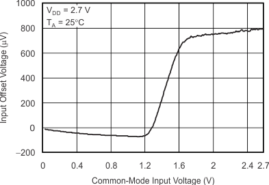 Figure 2. Input Offset Voltage vs Common-Mode Input Voltage
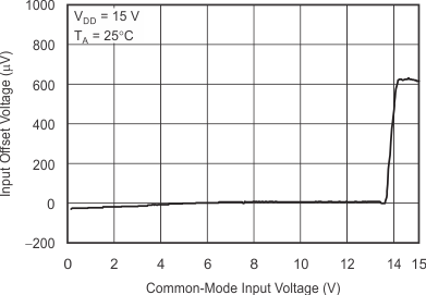 Figure 4. Input Offset Voltage vs Common-Mode Input Voltage
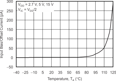 Figure 6. Input Bias or Offset Current vs Free-Air Temperature
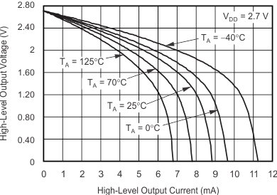 Figure 8. High-Level Output Voltage vs High-Level Output Current
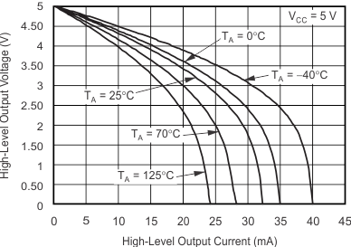 Figure 10. High-Level Output Voltage vs High-Level Output Current
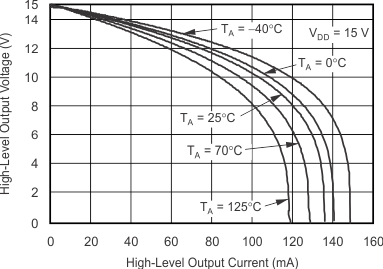 Figure 12. High-Level Output Voltage vs High-Level Output Current
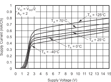 Figure 14. Supply Current vs Supply Voltage
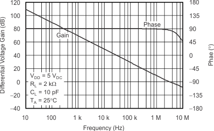 Figure 16. Differential Voltage Gain and Phase vs Frequency
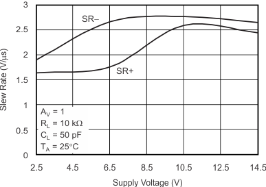 Figure 18. Slew Rate vs Supply Voltage
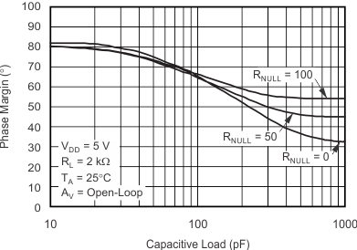 Figure 20. Phase Margin vs Capacitive Load
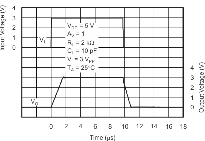 Figure 22. Voltage-Follower Large-Signal Pulse Response
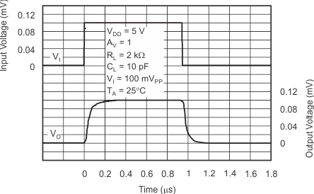 Figure 24. Voltage-Follower Small-Signal Pulse Response
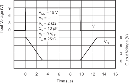 Figure 26. Inverting Large-Signal Response
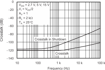 Figure 28. Crosstalk vs Frequency
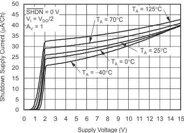 Figure 30. Shutdown Supply Current vs Supply Voltage
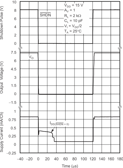 Figure 32. Shutdown Supply Current and Output Voltage vs Time
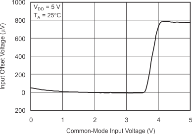 Figure 3. Input Offset Voltage vs Common-Mode Input Voltage
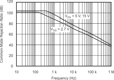 Figure 5. Common-Mode Rejection Ratio vs Frequency
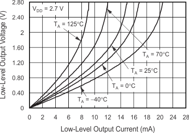 Figure 7. Low-Level Output Voltage vs Low-Level Output Current
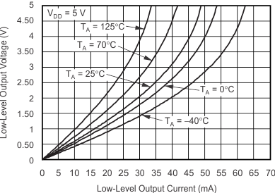 Figure 9. Low-Level Output Voltage vs Low-Level Output Current
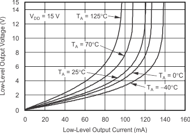 Figure 11. Low-Level Output Voltage vs Low-Level Output Current
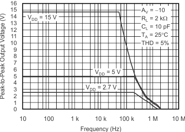 Figure 13. Peak-to-Peak Output Voltage vs Frequency
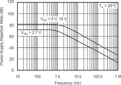 Figure 15. Power Supply Rejection Ratio vs Frequency
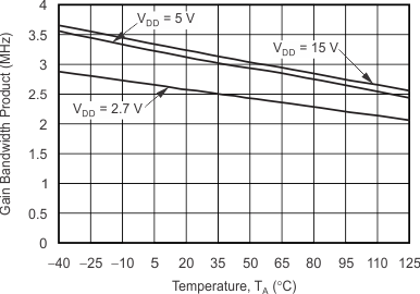 Figure 17. Gain Bandwidth Product vs Free-Air Temperature
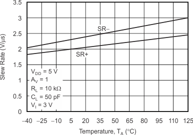 Figure 19. Slew Rate vs Free-Air Temperature
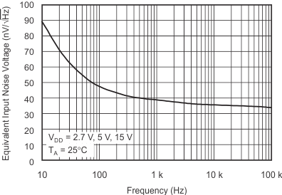 Figure 21. Equivalent Input Noise Voltage vs Frequency
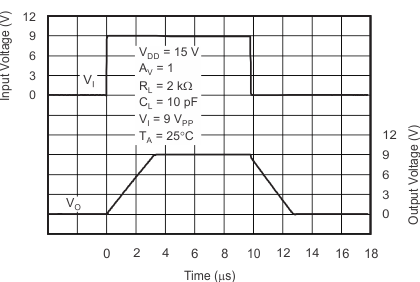 Figure 23. Voltage-Follower Large-Signal Pulse Response
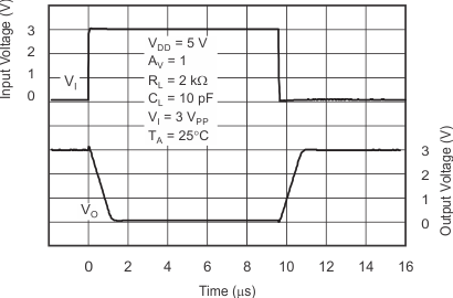 Figure 25. Inverting Large-Signal Response
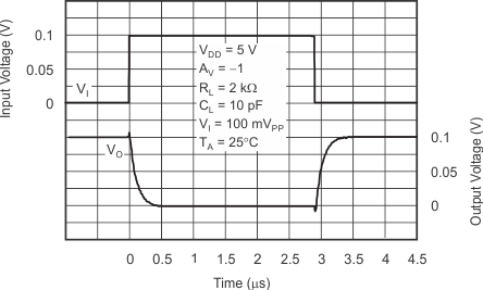 Figure 27. Inverting Small-Signal Response
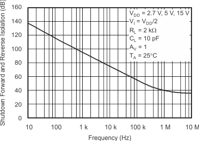 Figure 29. Shutdown Forward and Reverse Isolation vs Frequency
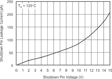 Figure 31. Shutdown Pin Leakage Current vs Shutdown Pin Voltage
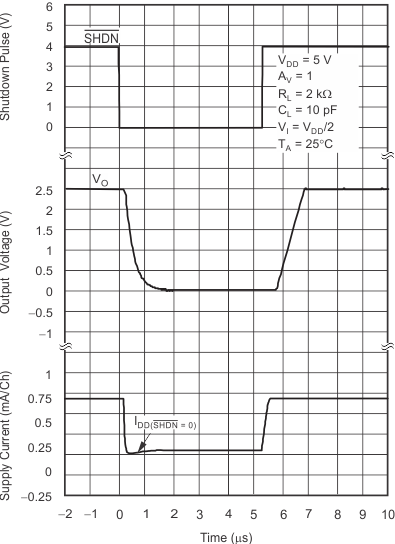 Figure 33. Shutdown Supply Current/output Voltage vs Time