SLAS355B December 2001 – December 2015 TLV2556
PRODUCTION DATA.
- 1 Features
- 2 Applications
- 3 Description
- 4 Revision History
- 5 Pin Configuration and Functions
-
6 Specifications
- 6.1 Absolute Maximum Ratings
- 6.2 ESD Ratings
- 6.3 Recommended Operating Conditions
- 6.4 Thermal Information
- 6.5 Electrical Characteristics
- 6.6 External Reference Specifications
- 6.7 Internal Reference Specifications
- 6.8 Operating Characteristics
- 6.9 Timing Requirements, VREF+ = 5 V
- 6.10 Timing Requirements, VREF+ = 2.5 V
- 6.11 Typical Characteristics
- 7 Parameter Measurement Information
-
8 Detailed Description
- 8.1 Overview
- 8.2 Functional Block Diagram
- 8.3
Feature Description
- 8.3.1 Converter Operation
- 8.3.2 Power Up and Initialization
- 8.3.3 Default Mode
- 8.3.4 Data Input
- 8.3.5 Data Input - Address/Command Bits
- 8.3.6 Data Output Length
- 8.3.7 LSB Out First
- 8.3.8 Bipolar Output Format
- 8.3.9 Reference
- 8.3.10 INT/EOC Output
- 8.3.11 Chip-Select Input (CS)
- 8.3.12 Power-Down Features
- 8.3.13 Analog MUX
- 8.4 Device Functional Modes
- 9 Application and Implementation
- 10Power Supply Recommendations
- 11Layout
- 12Device and Documentation Support
- 13Mechanical, Packaging, and Orderable Information
Package Options
Refer to the PDF data sheet for device specific package drawings
Mechanical Data (Package|Pins)
- DW|20
- PW|20
Thermal pad, mechanical data (Package|Pins)
Orderable Information
7 Parameter Measurement Information
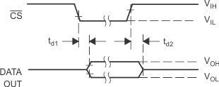 |
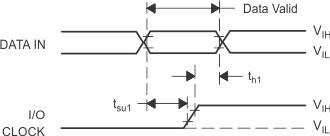 Figure 47. DATA IN and I/O CLOCK Voltage Figure 47. DATA IN and I/O CLOCK Voltage
|
 Waveforms |
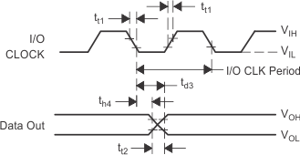 Figure 49. I/O CLOCK and DATA OUT Voltage Waveforms Figure 49. I/O CLOCK and DATA OUT Voltage Waveforms
|
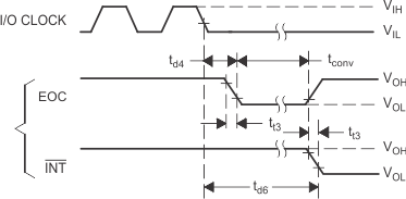 Figure 50. I/O CLOCK and EOC Voltage Waveforms Figure 50. I/O CLOCK and EOC Voltage Waveforms
|
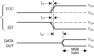 Figure 51. EOC and DATA OUT Voltage Waveforms Figure 51. EOC and DATA OUT Voltage Waveforms
|
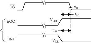 Figure 52. CS and EOC Waveforms Figure 52. CS and EOC Waveforms
|
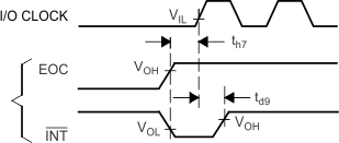 Figure 53. I/O CLOCK and EOC Voltage Waveforms Figure 53. I/O CLOCK and EOC Voltage Waveforms
|