SLOS922A September 2015 – December 2015 TLV27L2-Q1
PRODUCTION DATA.
- 1 Features
- 2 Applications
- 3 Description
- 4 Revision History
- 5 Selection Guide
- 6 Pin Configuration and Functions
- 7 Specifications
- 8 Detailed Description
- 9 Application and Implementation
- 10Power Supply Recommendations
- 11Layout
- 12Device and Documentation Support
- 13Mechanical, Packaging, and Orderable Information
Package Options
Mechanical Data (Package|Pins)
- D|8
Thermal pad, mechanical data (Package|Pins)
Orderable Information
9 Application and Implementation
NOTE
Information in the following applications sections is not part of the TI component specification, and TI does not warrant its accuracy or completeness. TI’s customers are responsible for determining suitability of components for their purposes. Customers should validate and test their design implementation to confirm system functionality.
9.1 Application Information
9.1.1 General Configurations
When receiving low-level signals, limiting the bandwidth of the incoming signals into the system is often required. The simplest way limit the bandwidth is to place an RC filter at the noninverting terminal of the amplifier as shown in Figure 26.
 Figure 26. Single-Pole Low-Pass Filter
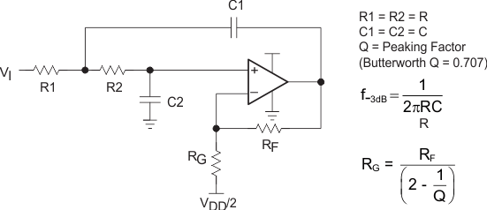
If even more attenuation is required, a multiple pole filter is required. The Sallen-Key filter can be used for this task. For best results, the amplifier should have a bandwidth that is 8 to 10 times the filter frequency bandwidth. Failure to do select an amplifier with an appropriate bandwidth can result in phase shift of the amplifier.
 Figure 27. 2-Pole Low-Pass Sallen-Key Filter
9.2 Typical Application
This single-supply low-side, bi-directional current sensing solution can accurately detect load currents from –1 A to +1 A. The linear range of the output is from 110 mV to 3.19 V. The design uses the TLV27L2-Q1 device configured as a difference amplifier and reference voltage buffer.
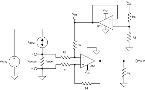
Low-side current sensing is desirable because the common-mode voltage is near ground. Therefore the current sensing solution is independent of the bus voltage, VBUS. When sensing bidirectional currents, a reference voltage must be added to differentiate between positive and negative currents. Figure 28 shows a general circuit topology for a low-side, bidirectional current-sensing solution. This topology is particularly useful when cost is a priority at the expense of accuracy and printed circuit board (PCB) space. The shunt voltage (VSHUNT) is created by the load current (ILOAD) flowing through the shunt resistor (RSHUNT). The VSHUNT voltage is amplified by an op amp (U1A) according to the gain set by the ratio of R4 to R3. To achieve the transfer function in Equation 1 and to minimize errors, set R4 equal to R2 and R3 equal to R1. To provide the reference voltage in this design, divide down the supply voltage (VCC) using R5 and R6. The reference voltage is then buffered using an additional op amp (U1B).
 Figure 28. Application Schematic ±1-A Single-Supply Low-Side Current Sensing Solution
9.2.1 Design Requirements
The design requirements are as follows:
Supply voltage: 3.3 V
Input: –1 A to +1 A
Output: 110 mV to 3.19 V
Maximum shunt voltage: ±100 mV
9.2.2 Detailed Design Procedure
9.2.2.1 Shunt Resistor (RSHUNT)
As shown in Figure 28, the value of VSHUNT is the ground potential for the system load. If the value of VSHUNT is too large, it can cause issues when interfacing with systems with a true ground potential of 0 V. If the value of VSHUNT is too negative, it can violate the input common-mode voltage of the differential amplifier in addition to potential interfacing issues. Therefore, limit the voltage across the shunt resistor. Use Equation 2 to calculate the maximum value of RSHUNT given a maximum shunt voltage of 100 mV.

Because cost is a priority in this design, a shunt resistor with a 0.5% tolerance was selected.
9.2.2.2 Operational Amplifiers
The shunt voltage in this design can range from –100 mV to +100 mV. The shut voltage is divided down by the resistors, R1 and R2. The op amp configured as a difference amplifier (U1A) must have an input common-mode that includes this voltage range. Therefore an op amp with rail-to-rail input (RRI) that extends below V– is recommended. The output swing of the amplifier should also be rail-to-rail output (RRO) to maximize the dynamic range of the system. Use of a CMOS op amp is recommended because the supply voltage is 3.3 V. The supply-splitter op amp (U1B) should have low offset voltage. Because this design includes two op amps, a dual package minimizes the required area. This design uses the TLV27L2-Q1 device because it is a RRO CMOS device. In addition, the cost versus performance of the device is excellent.
9.2.2.3 Reference Voltage Resistors (R5-R6)
Because the load current range is symmetric (–1 A to +1 A), the resistors that divide down the supply voltage should be equal so that the reference voltage is the mid supply ([(V+) – (V–)] / 2 or, for this example, (3.3 V – 0 V) / 2 = 1.65 V). Because cost is a priority in this design, the tolerance should be consistent with the shunt resistor tolerance (0.5%). Finally, select resistors that are large enough to meet the power consumption requirement of the system. For this design, 10-kΩ resistors were selected.
9.2.2.4 Difference Amplifier Gain Setting Resistors (R1-R4)
Equation 3 and Equation 4 show the input common-mode (VCM) and output voltage range (VOUT) of the TLV27L2-Q1 device given a 3.3-V supply.
Use Equation 5 to calculate the gain.

The selected value for the R1 and R3 resistors was 1 kΩ. The selected value for the R2 and R4 resistors was 15.4 kΩ, which is the nearest 0.1% value to the ideal value of 15.5 kΩ. Therefore, the ideal gain of the difference amplifier is 15.4 V/V.
9.2.3 Application Curve
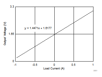
Figure 29 shows the measured transfer function of the design.
