SBOS300C february   2004  – april 2023 TLV3011 , TLV3011B , TLV3012 , TLV3012B

PRODUCTION DATA  

  1. Features
  2. Applications
  3. Description
  4. Revision History
  5. Pin Configuration and Functions
  6. Specifications
    1. 6.1  Absolute Maximum Ratings- TLV3011 and TLV3012
    2. 6.2  Absolute Maximum Ratings - TLV3011B and TLV3012B
    3. 6.3  ESD Ratings
    4. 6.4  Thermal Information - TLV3011 and TLV3012
    5. 6.5  Thermal Information- TLV3011B and TLV3012B
    6. 6.6  Recommended Operating Conditions
    7. 6.7  Electrical Characteristics - TLV3011 and TLV3012
    8. 6.8  Switching Characteristics - TLV3011 and TLV3012
    9. 6.9  Electrical Characteristics - TLV3011B and TLV3012B
    10. 6.10 Switching Characteristics - TLV3011B and TLV3012B
  7. Typical Characteristics - TLV3011 and TLV3012
  8. Typical Characteristics - TLV3011B and TLV3012B
  9. Detailed Description
    1. 9.1 Overview
    2. 9.2 Functional Block Diagram
    3. 9.3 Feature Description
    4. 9.4 Device Functional Modes
      1. 9.4.1 Open Drain Output (TLV3011 and TLV3011B)
      2. 9.4.2 Push-Pull Output (TLV3012 and TLV3012B)
      3. 9.4.3 Voltage Reference
      4. 9.4.4 TLV3011B and TLV3012B Fail-Safe inputs
      5. 9.4.5 TLV3011B and TLV3012B Power On Reset
  10. 10Application and Implementation
    1. 10.1 Application Information
      1. 10.1.1 External Hysteresis
      2. 10.1.2 TLV3011B and TLV3012B Hysteresis
    2. 10.2 Typical Application
      1. 10.2.1 Under-Voltage Detection
        1. 10.2.1.1 Design Requirements
        2. 10.2.1.2 Detailed Design Procedure
        3. 10.2.1.3 Application Curve
    3. 10.3 System Examples
      1. 10.3.1 Power-On Reset
      2. 10.3.2 Relaxation Oscillator
    4. 10.4 Power Supply Recommendations
    5. 10.5 Layout
      1. 10.5.1 Layout Guidelines
      2. 10.5.2 Layout Example
  11. 11Device and Documentation Support
    1. 11.1 Receiving Notification of Documentation Updates
    2. 11.2 Support Resources
    3. 11.3 Trademarks
    4. 11.4 Electrostatic Discharge Caution
    5. 11.5 Glossary
  12. 12Mechanical, Packaging, and Orderable Information

Package Options

Mechanical Data (Package|Pins)
Thermal pad, mechanical data (Package|Pins)
Orderable Information

Typical Characteristics - TLV3011 and TLV3012

At TA = 25°C, VS = 1.8 V to 5.5 V, and Input Overdrive = 100 mV, unless otherwise noted.

GUID-160BCE02-610D-477F-8FCB-D97ED884C5A9-low.gif
Figure 7-1 Quiescent Current vs Temperature
GUID-2A57FF46-4BF2-497E-8D41-93ED412B36F1-low.gif
Figure 7-3 Input Bias Current vs Temperature
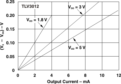
GUID-E6059638-75D6-42F6-B5D7-34116A38ED85-low.gif
Figure 7-5 Output High vs Output Current
GUID-C0AA13FE-4138-40FB-A695-7ED3F10D7B88-low.gif
Figure 7-7 Propagation Delay (tPHL) vs Capacitive Load
GUID-87656ADC-B5ED-4ED8-AA53-BAEE766D270F-low.gif
Figure 7-9 Propagation Delay (tPHL) vs Input Overdrive
GUID-50DCE9E4-20D1-49ED-A099-9308E718B2E5-low.gif
Figure 7-11 Propagation Delay (tPHL) vs Temperature
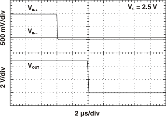
GUID-F403A978-93B5-4825-9858-2073250B21B5-low.gif
Figure 7-13 Propagation Delay (tPHL)
GUID-9AB3E974-DCFE-426B-B18E-2238E691F543-low.gif
Figure 7-15 Propagation Delay (tPHL)
GUID-4668633F-3471-4950-A16F-ED32659866A8-low.gif
Figure 7-17 Reference Voltage vs Output Load Current (Sinking)
GUID-017AFCDE-B98C-4BFE-80E6-5357BCC71D7F-low.gif
Figure 7-19 Short-Circuit Current vs Supply Voltage
GUID-96017E1D-FF89-4F15-82E0-513708D1AA7F-low.gif
Figure 7-2 Quiescent Current vs Output Switching Frequency
GUID-86AEA965-6F2B-46AA-A0CC-27D407385152-low.gif
Figure 7-4 Output Low vs Output Current
GUID-8D85A692-6390-46D3-A4E6-BAF67AC999F3-low.gif
Figure 7-6 Propagation Delay (tPLH) vs Capacitive Load
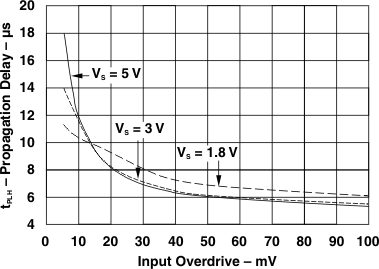
GUID-D496714A-36E8-4033-832E-5ACC948F4D9B-low.gif
Figure 7-8 Propagation Delay (tPLH) vs Input Overdrive
GUID-B4FBDE70-CED8-413C-8839-428B50BB1C2F-low.gif
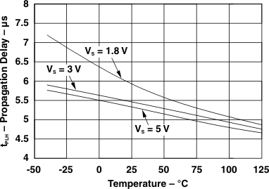
Figure 7-10 Propagation Delay (tPLH) vs Temperature
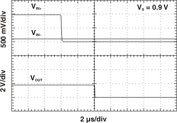
GUID-E1794A61-F1DF-443E-B791-5B205CA77D1D-low.gif
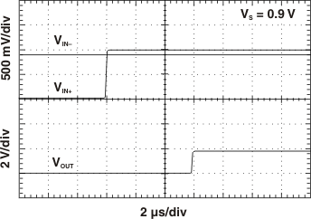
Figure 7-12 Propagation Delay (tPLH)
GUID-90C32444-4195-408E-AD8A-6A763F817125-low.gif
Figure 7-14 Propagation Delay (tPLH)
GUID-D68B9AD8-8291-4D1F-9FEE-6D42B16099EF-low.gif
Figure 7-16 Reference Voltage vs Output Load Current (Sourcing)
GUID-98F34834-D82A-4F9C-83A4-F9778AC2CB76-low.gif
Figure 7-18 Reference Voltage vs Temperature
GUID-0461D2A6-9C5B-4363-9BCE-BB182D7D48D3-low.gif
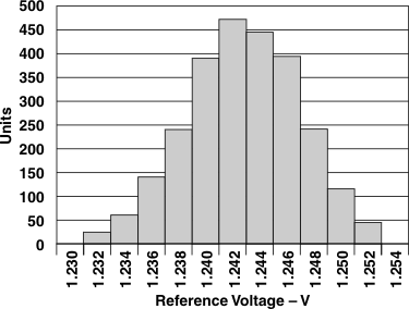
Figure 7-20 Reference Voltage Distribution