SGLS349A october 2006 – may 2023 TLV3011-EP , TLV3012-EP
PRODUCTION DATA
- 1
- 1 Features
- 2 Applications
- 3 Description
- 4 Revision History
- 5 Pin Configuration and Functions
-
6 Specifications
- 6.1 Absolute Maximum Ratings - TLV3011-EP
- 6.2 Absolute Maximum Ratings - TLV3012-EP
- 6.3 ESD Ratings
- 6.4 Thermal Resistance Characteristics
- 6.5 Recommended Operating Conditions - TLV3011-EP
- 6.6 Recommended Operating Conditions - TLV3012-EP
- 6.7 Electrical Characteristics - TLV3011-EP
- 6.8 Electrical Characteristics - TLV3012-EP
- 6.9 Switching Characteristics - TLV3012-EP
- 6.10 Typical Characteristics - TLV3011-EP
- 6.11 Typical Characteristics - TLV3012-EP
- 7 Detailed Description
- 8 Application and Implementation
- 9 Device and Documentation Support
- 10Mechanical, Packaging, and Orderable Information
Package Options
Refer to the PDF data sheet for device specific package drawings
Mechanical Data (Package|Pins)
- DBV|6
Thermal pad, mechanical data (Package|Pins)
Orderable Information
8.1.1 External Hysteresis
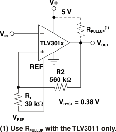
Comparator inputs have no noise immunity within the range of specified offset voltage (±12 mV). For noisy input signals, the comparator output may display multiple switching as input signals move through the switching threshold. The typical comparator threshold of the TLV301x-EP is ±0.5 mV. To prevent multiple switching within the comparason threshold of the comparator, external hysteresis may be added by connecting a small amount of feedback to the positive input. Figure 8-2 shows a typical topology used to introduce hysteresis, described by this equation:

 Figure 8-2 Adding Hysteresis
VHYST sets the value of the transition voltage required to switch the comparator output by increasing the threshold region, thereby reducing sensitivity to noise.