SBOS300C february 2004 – april 2023 TLV3011 , TLV3011B , TLV3012 , TLV3012B
PRODUCTION DATA
- 1 Features
- 2 Applications
- 3 Description
- 4 Revision History
- 5 Pin Configuration and Functions
-
6 Specifications
- 6.1 Absolute Maximum Ratings- TLV3011 and TLV3012
- 6.2 Absolute Maximum Ratings - TLV3011B and TLV3012B
- 6.3 ESD Ratings
- 6.4 Thermal Information - TLV3011 and TLV3012
- 6.5 Thermal Information- TLV3011B and TLV3012B
- 6.6 Recommended Operating Conditions
- 6.7 Electrical Characteristics - TLV3011 and TLV3012
- 6.8 Switching Characteristics - TLV3011 and TLV3012
- 6.9 Electrical Characteristics - TLV3011B and TLV3012B
- 6.10 Switching Characteristics - TLV3011B and TLV3012B
- 7 Typical Characteristics - TLV3011 and TLV3012
- 8 Typical Characteristics - TLV3011B and TLV3012B
- 9 Detailed Description
- 10Application and Implementation
- 11Device and Documentation Support
- 12Mechanical, Packaging, and Orderable Information
Package Options
Mechanical Data (Package|Pins)
Thermal pad, mechanical data (Package|Pins)
Orderable Information
10.1 Application Information
The TLV301x and TLV301xB comparator family with on-chip 1.242-V series reference with the choice of either open-drain or push-pull output stages.
A typical supply current of 2.4 μA and small packaging combine with 1.65-V supply requirements to make the TLV301xB devices optimal for battery and portable designs.
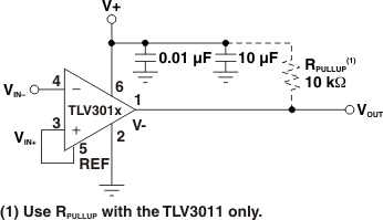
Figure 10-1 shows the typical connections for the TLV3012 device.
 Figure 10-1 Basic Connections