SBOS561C March   2012  – May 2024 TLV3201 , TLV3202

PRODMIX  

  1.   1
  2. Features
  3. Applications
  4. Description
  5. Device Comparison Table
  6. Pin Configuration and Functions
    1.     Pin Functions: TLV3201
    2.     Pin Functions: TLV3202
  7. Specifications
    1. 6.1 Absolute Maximum Ratings
    2. 6.2 ESD Ratings
    3. 6.3 Recommended Operating Conditions
    4. 6.4 Thermal Information
    5. 6.5 Electrical Characteristics: VCC = 5V
    6. 6.6 Switching Characteristics: VCC = 5V
    7. 6.7 Electrical Characteristics: VCC = 2.7V
    8. 6.8 Switching Characteristics: VCC = 2.7V
    9. 6.9 Typical Characteristics
  8. Detailed Description
    1. 7.1 Overview
    2. 7.2 Functional Block Diagram
    3. 7.3 Feature Description
      1. 7.3.1 Operating Voltage
      2. 7.3.2 Input Overvoltage Protection
    4. 7.4 Device Functional Modes
  9. Application and Implementation
    1. 8.1 Application Information
      1. 8.1.1 Comparator Inputs
      2. 8.1.2 External Hysteresis
        1. 8.1.2.1 Inverting Comparator with Hysteresis
        2. 8.1.2.2 Noninverting Comparator With Hysteresis
      3. 8.1.3 Capacitive Loads
    2. 8.2 Typical Applications
      1. 8.2.1 TLV3201 Configured as an AC-Coupled Comparator
        1. 8.2.1.1 Design Requirements
        2. 8.2.1.2 Detailed Design Procedure
        3. 8.2.1.3 Application Curve
      2. 8.2.2 TLV3201 and OPA320 Configured as a Fast-Response Output Current Monitor
      3. 8.2.3 TLV3201 and TMP20 Configured as a Precision Analog Temperature Switch
    3. 8.3 Power Supply Recommendations
    4. 8.4 Layout
      1. 8.4.1 Layout Guidelines
      2. 8.4.2 Layout Example
  10. Device and Documentation Support
    1. 9.1 Device Support
      1. 9.1.1 Development Support
        1. 9.1.1.1 TINA-TI™ (Free Software Download)
        2. 9.1.1.2 Universal Op Amp EVM
        3. 9.1.1.3 TI Precision Designs
        4. 9.1.1.4 WEBENCH Filter Designer
    2. 9.2 Documentation Support
      1. 9.2.1 Related Documentation
    3. 9.3 Receiving Notification of Documentation Updates
    4. 9.4 Support Resources
    5. 9.5 Trademarks
    6. 9.6 Electrostatic Discharge Caution
    7. 9.7 Glossary
  11. 10Revision History
  12. 11Mechanical, Packaging, and Orderable Information

Package Options

Mechanical Data (Package|Pins)
Thermal pad, mechanical data (Package|Pins)
Orderable Information

Noninverting Comparator With Hysteresis

A noninverting comparator with hysteresis requires a two-resistor network, as shown in Figure 8-5, and a voltage reference (VREF) at the inverting input. When VIN is low, the output is also low. For the output to switch from low to high, VIN must rise up to VIN1. VIN1 is calculated by Equation 4.

Equation 4. TLV3201 TLV3202

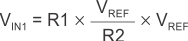
When VIN is high, the output is also high. In order for the comparator to switch back to a low state, VIN must equal VREF before VA is again equal to VREF. VIN can be calculated by Equation 5.

Equation 5. TLV3201 TLV3202

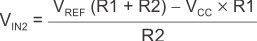
The hysteresis of this circuit is the difference between VIN1 and VIN2, as defined by Equation 6.

Equation 6. TLV3201 TLV3202
TLV3201 TLV3202 TLV3201 in Noninverting Configuration With Hysteresis
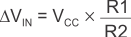
Figure 8-5 TLV3201 in Noninverting Configuration With Hysteresis