SBOS856A February 2017 – December 2017 TLV3201-Q1 , TLV3202-Q1
PRODUCTION DATA.
- 1 Features
- 2 Applications
- 3 Description
- 4 Revision History
- 5 Device Comparison Table
- 6 Pin Configuration and Functions
- 7 Specifications
- 8 Detailed Description
- 9 Application and Implementation
- 10Power Supply Recommendations
- 11Layout
- 12Device and Documentation Support
- 13Mechanical, Packaging, and Orderable Information
Package Options
Mechanical Data (Package|Pins)
- DGK|8
Thermal pad, mechanical data (Package|Pins)
Orderable Information
7 Specifications
7.1 Absolute Maximum Ratings
over operating free-air temperature range (unless otherwise noted)(1)| MIN | MAX | UNIT | ||
|---|---|---|---|---|
| Voltage | Supply voltage | 7 | V | |
| Signal input pins(2) | –0.5 | (VCC) + 0.5 | ||
| Current | Signal input pins(2) | –10 | 10 | mA |
| Output short circuit(3) | 100 | |||
| Temperature | Operating | –55 | 125 | °C |
| Junction, TJ | 150 | |||
| Storage, Tstg | –65 | 150 | ||
(1) Stresses beyond those listed under Absolute Maximum Ratings may cause permanent damage to the device. These are stress ratings only, which do not imply functional operation of the device at these or any other conditions beyond those indicated under Recommended Operating Conditions. Exposure to absolute-maximum-rated conditions for extended periods may affect device reliability.
(2) Input pins are diode-clamped to the power-supply rails. Input signals that can swing more than 0.5 V beyond the supply rails must be current limited to 10 mA or less.
(3) Short-circuit to ground.
7.2 ESD Ratings
| VALUE | UNIT | |||
|---|---|---|---|---|
| TLV3201-Q1 | ||||
| V(ESD) | Electrostatic discharge | Human-body model (HBM), per AEC Q100-002(1) | ±3000 | V |
| Charged-device model (CDM), per AEC Q100-011 | ±750 | |||
| TLV3202-Q1 | ||||
| V(ESD) | Electrostatic discharge | Human-body model (HBM), per AEC Q100-002(1) | ±4000 | V |
| Charged-device model (CDM), per AEC Q100-011 | ±750 | |||
(1) AEC Q100-002 indicates that HBM stressing shall be in accordance with the ANSI/ESDA/JEDEC JS-001 specification.
7.3 Recommended Operating Conditions
over operating free-air temperature range (unless otherwise noted)| MIN | MAX | UNIT | ||
|---|---|---|---|---|
| VS | Supply voltage, VS = (VS+) – (VS–) | 2.7 (±1.35) | 5.5 (±2.75) | V |
| TA | Specified temperature | –40 | 125 | °C |
7.4 Thermal Information
| THERMAL METRIC(1) | TLV3201-Q1 | TLV3202-Q1 | UNIT | |||
|---|---|---|---|---|---|---|
| DCK (SC-70) | DGK (VSSOP) | |||||
| 5 PINS | 8 PINS | |||||
| RθJA | Junction-to-ambient thermal resistance | 281.9 | 201.9 | °C/W | ||
| RθJC(top) | Junction-to-case (top) thermal resistance | 97.6 | 92.5 | °C/W | ||
| RθJB | Junction-to-board thermal resistance | 68.3 | 123.3 | °C/W | ||
| ψJT | Junction-to-top characterization parameter | 2.6 | 23 | °C/W | ||
| ψJB | Junction-to-board characterization parameter | 67.3 | 212.6 | °C/W | ||
(1) For more information about traditional and new thermal metrics, see the Semiconductor and IC Package Thermal Metrics application report.
7.5 Electrical Characteristics: VCC = 5 V
at TA = 25°C and VCC = 5 V (unless otherwise noted)| PARAMETER | TEST CONDITIONS | MIN | TYP | MAX | UNIT | ||
|---|---|---|---|---|---|---|---|
| OFFSET VOLTAGE | |||||||
| VIO | Input offset voltage | VCM = VCC / 2 | 1 | 5 | mV | ||
| TA = –40°C to 125°C | 6 | ||||||
| dVOS/dT | Input offset voltage drift | TA = –40°C to 125°C | 1 | 10 | µV/°C | ||
| PSRR | Power-supply rejection ratio | VCM = VCC / 2, VCC = 2.5 V to 5.5 V | 65 | 85 | dB | ||
| Input hysteresis | 1.2 | mV | |||||
| INPUT BIAS CURRENT | |||||||
| IIB | Input bias current | VCM = VCC / 2 | 1 | 50 | pA | ||
| TA = –40°C to 125°C | 5 | nA | |||||
| IIO | Input offset current | VCM = VCC / 2 | 1 | 50 | pA | ||
| TA = –40°C to 125°C | 2.5 | nA | |||||
| INPUT VOLTAGE RANGE | |||||||
| VCM | Common-mode voltage | TA = –40°C to 125°C | (VEE) – 0.2 | (VCC) + 0.2 | V | ||
| CMRR | Common-mode rejection ratio | –0.2 V < VCM < 5.2 V | 60 | 70 | dB | ||
| INPUT IMPEDANCE | |||||||
| Common mode | 1013 || 2 | Ω || pF | |||||
| Differential | 1013 || 4 | Ω || pF | |||||
| OUTPUT | |||||||
| VOL | Voltage output swing from lower rail | ISINK = 4 mA | 175 | 190 | mV | ||
| TA = –40°C to 125°C | 225 | ||||||
| VOH | Voltage output swing from upper rail | ISOURCE = 4 mA | 120 | 140 | mV | ||
| TA = –40°C to 125°C | 170 | ||||||
| ISC | Short-circuit current (per comparator) | ISC sinking | 40 | 48 | mA | ||
| TA = –40°C to 125°C | See Figure 14 | ||||||
| ISC sourcing | 52 | 60 | |||||
| TA = –40°C to 125°C | See Figure 14 | ||||||
| POWER SUPPLY | |||||||
| VCC | Specified voltage | 2.7 | 5.5 | V | |||
| IQ | Quiescent current | TA = 25°C | 40 | 50 | µA | ||
| TA = –40°C to 125°C | 65 | ||||||
7.6 Electrical Characteristics: VCC = 2.7 V
at TA = 25°C and VCC = 2.7 V (unless otherwise noted)| PARAMETER | TEST CONDITIONS | MIN | TYP | MAX | UNIT | ||
|---|---|---|---|---|---|---|---|
| OFFSET VOLTAGE | |||||||
| VIO | Input offset voltage | VCM = VCC / 2 | 1 | 5 | mV | ||
| TA = –40°C to 125°C | 6 | ||||||
| dVOS/dT | Input offset voltage drift | TA = –40°C to 125°C | 1 | 10 | µV/°C | ||
| PSRR | Power-supply rejection ratio | VCM = VCC / 2, VCC = 2.5 V to 5.5 V | 65 | 85 | dB | ||
| Input hysteresis | 1.2 | mV | |||||
| INPUT BIAS CURRENT | |||||||
| IIB | Input bias current | VCM = VCC / 2 | 1 | 50 | pA | ||
| TA = –40°C to 125°C | 5 | nA | |||||
| IIO | Input offset current | VCM = VCC / 2 | 1 | 50 | pA | ||
| TA = –40°C to 125°C | 2.5 | nA | |||||
| INPUT VOLTAGE RANGE | |||||||
| VCM | Common-mode voltage | TA = –40°C to 125°C | (VEE) – 0.2 | (VCC) + 0.2 | V | ||
| CMRR | Common-mode rejection ratio | –0.2 V < VCM < 2.9 V | 56 | 68 | dB | ||
| INPUT IMPEDANCE | |||||||
| Common mode | 1013 || 2 | Ω || pF | |||||
| Differential | 1013 || 4 | Ω || pF | |||||
| OUTPUT | |||||||
| VOL | Voltage output swing from lower rail | ISINK = 4 mA | 230 | 260 | mV | ||
| TA = –40°C to 125°C | 325 | ||||||
| VOH | Voltage output swing from upper rail | ISOURCE = 4 mA | 210 | 250 | mV | ||
| TA = –40°C to 125°C | 350 | ||||||
| ISC | Short-circuit current (per comparator) | ISC sinking | 13 | 19 | mA | ||
| TA = –40°C to 125°C | See Figure 14 | ||||||
| ISC sourcing | 15 | 21 | |||||
| TA = –40°C to 125°C | See Figure 14 | ||||||
| POWER SUPPLY | |||||||
| VCC | Specified voltage | 2.7 | 5.5 | V | |||
| IQ | Quiescent current | TA = 25°C | 36 | 46 | µA | ||
| TA = –40°C to 125°C | 60 | ||||||
7.7 Switching Characteristics
over operating free-air temperature range (unless otherwise noted)| PARAMETER | TEST CONDITIONS | MIN | TYP | MAX | UNIT | |||
|---|---|---|---|---|---|---|---|---|
| tPD | Propagation delay time | Low to high | Input overdrive = 20 mV, CL = 15 pF | 47 | 50 | ns | ||
| Input overdrive = 100 mV, CL = 15 pF | 42 | 50 | ||||||
| TA = –40°C to 125°C | 55 | |||||||
| High to low | Input overdrive = 20 mV, CL = 15 pF | 40 | 50 | |||||
| Input overdrive = 100 mV, CL = 15 pF | 38 | 50 | ||||||
| TA = –40°C to 125°C | 55 | |||||||
| Propagation delay skew | Input overdrive = 20 mV, CL = 15 pF | 2 | ns | |||||
| Propagation delay matching (TLV3202-Q1) | High to low or low to high, input overdrive = 20 mV, CL = 15 pF | 5 | ns | |||||
| tR | Rise time | 10% to 90% | 2.9 | ns | ||||
| tF | Fall time | 10% to 90% | 3.7 | ns | ||||
7.8 Typical Characteristics
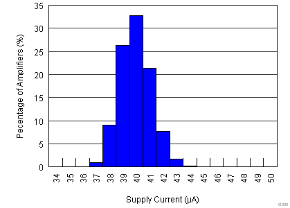
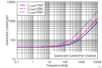
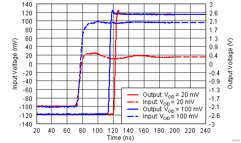
at TA = 25°C, VCC = 5 V, and input overdrive (VOD) = 20 mV (unless otherwise noted)


Power-Supply Rejection Ratio vs Temperature

vs Common-Mode Input Voltage


vs Temperature

vs Common-Mode Input Voltage


