SBOS561C March 2012 – May 2024 TLV3201 , TLV3202
PRODMIX
- 1
- 1 Features
- 2 Applications
- 3 Description
- 4 Device Comparison Table
- 5 Pin Configuration and Functions
- 6 Specifications
- 7 Detailed Description
- 8 Application and Implementation
- 9 Device and Documentation Support
- 10Revision History
- 11Mechanical, Packaging, and Orderable Information
Package Options
Mechanical Data (Package|Pins)
Thermal pad, mechanical data (Package|Pins)
Orderable Information
8.1.2.1 Inverting Comparator with Hysteresis
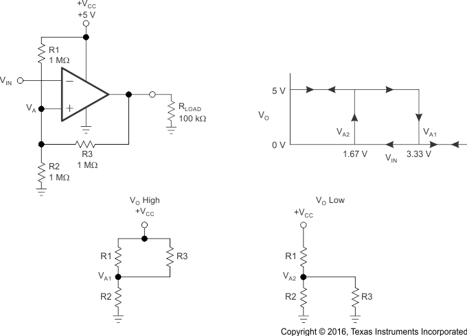
The inverting comparator with hysteresis requires a three-resistor network that is referenced to the comparator supply voltage (VCC), as shown in Figure 8-4. When VIN at the inverting input is less than VA, the output voltage is high (for simplicity, assume VO switches as high as VCC). The three network resistors can be represented as R1 || R3 in series with R2. The lower input trip voltage (VA1) is defined by Equation 1.

When VIN is greater than [VA × (VIN > VA)], the output voltage is low, very close to ground. In this case, the three network resistors can be presented as R2 || R3 in series with R1. The upper trip voltage (VA2) is defined by Equation 2.

The total hysteresis provided by the network is defined by Equation 3.

 Figure 8-4 TLV3201 in Inverting Configuration With Hysteresis