SLAS715D June 2010 – October 2024 TLV320AIC3104-Q1
PRODUCTION DATA
- 1
- 1 Features
- 2 Applications
- 3 Description
- 4 Device Comparison
- 5 Pin Configuration and Functions
-
6 Specifications
- 6.1 Absolute Maximum Ratings
- 6.2 ESD Ratings
- 6.3 Recommended Operating Conditions
- 6.4 Thermal Information
- 6.5 Electrical Characteristics
- 6.6 Switching Characteristics I2S/LJF/RJF Timing in Master Mode
- 6.7 Switching Characteristics I2S/LJF/RJF Timing in Slave Mode
- 6.8 Switching Characteristics DSP Timing in Master Mode
- 6.9 Switching Characteristics DSP Timing in Slave Mode
- 6.10 Typical Characteristics
-
7 Detailed Description
- 7.1 Overview
- 7.2 Functional Block Diagram
- 7.3
Feature Description
- 7.3.1 Audio Data Converters
- 7.3.2 Stereo Audio ADC
- 7.3.3 Automatic Gain Control (AGC)
- 7.3.4 Stereo Audio DAC
- 7.3.5 Digital Audio Processing for Playback
- 7.3.6 Digital Interpolation Filter
- 7.3.7 Delta-Sigma Audio DAC
- 7.3.8 Audio DAC Digital Volume Control
- 7.3.9 Analog Output Common-mode Adjustment
- 7.3.10 Audio DAC Power Control
- 7.3.11 Audio Analog Inputs
- 7.3.12 Analog Input Bypass Path Functionality
- 7.3.13 ADC PGA Signal Bypass Path Functionality
- 7.3.14 Input Impedance and VCM Control
- 7.3.15 MICBIAS Generation
- 7.3.16 Analog Fully Differential Line Output Drivers
- 7.3.17 Analog High-Power Output Drivers
- 7.3.18 Short-Circuit Output Protection
- 7.3.19 Jack and Headset Detection
- 7.4 Device Functional Modes
- 7.5 Programming
- 8 Register Maps
- 9 Application and Implementation
- 10Device and Documentation Support
- 11Revision History
- 12Mechanical, Packaging, and Orderable Information
Package Options
Mechanical Data (Package|Pins)
- RHB|32
Thermal pad, mechanical data (Package|Pins)
- RHB|32
Orderable Information
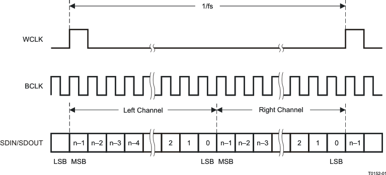
7.5.8 DSP Mode
In DSP mode, the rising edge of the word clock starts the data transfer with the left-channel data first, immediately followed by the right-channel data. Each data bit is valid on the falling edge of the bit clock.
 Figure 7-19 DSP Serial Data Bus Mode Operation