SLAS663C August 2009 – June 2016 TLV320AIC3106-Q1
PRODUCTION DATA.
- 1 Features
- 2 Applications
- 3 Description
- 4 Revision History
- 5 Description (Continued)
- 6 Device Comparison Table
- 7 Pin Configuration and Functions
-
8 Specifications
- 8.1 Absolute Maximum Ratings
- 8.2 ESD Ratings
- 8.3 Recommended Operating Conditions
- 8.4 Thermal Information
- 8.5 Electrical Characteristics
- 8.6 Switching Characteristics I2S/LJF/RJF In Master Mode
- 8.7 Switching Characteristics I2S/LJF/RJF In Slave Mode
- 8.8 Switching Characteristics DSP In Master Mode
- 8.9 Switching Characteristics DSP In Slave Mode
- 8.10 Typical Characteristics
-
9 Detailed Description
- 9.1 Overview
- 9.2 Functional Block Diagram
- 9.3
Feature Description
- 9.3.1 Audio Data Converters
- 9.3.2 Stereo Audio ADC
- 9.3.3 Automatic Gain Control (AGC)
- 9.3.4 Stereo Audio DAC
- 9.3.5 Digital Audio Processing For Playback
- 9.3.6 Digital Interpolation Filter
- 9.3.7 Delta-Sigma Audio Dac
- 9.3.8 Audio Dac Digital Volume Control
- 9.3.9 Analog Output Common-Mode Adjustment
- 9.3.10 Audio DAC Power Control
- 9.3.11 Audio Analog Inputs
- 9.3.12 Analog Input Bypass Path Functionality
- 9.3.13 ADC PGA Signal Bypass Path Functionality
- 9.3.14 Input Impedance and VCM Control
- 9.3.15 MICBIAS Generation
- 9.3.16 Analog Fully Differential Line Output Drivers
- 9.3.17 Analog High Power Output Drivers
- 9.3.18 Short Circuit Output Protection
- 9.3.19 Jack and Headset Detection
- 9.3.20 General-Purpose I/O
- 9.4 Device Functional Modes
- 9.5
Programming
- 9.5.1 Hardware Reset
- 9.5.2 Digital Control Serial Interface
- 9.5.3 I2C Control Mode
- 9.5.4 I2C Bus Debug In A Glitched System
- 9.5.5 Digital Audio Data Serial Interface
- 9.5.6 Right-Justified Mode
- 9.5.7 Left-Justified Mode
- 9.5.8 I2S Mode
- 9.5.9 DSP Mode
- 9.5.10 TDM Data Transfer
- 9.5.11 Audio Clock Generation
- 9.6 Register Maps
- 10Application and Implementation
- 11Power Supply Recommendations
- 12Layout
- 13Device and Documentation Support
- 14Mechanical, Packaging, And Orderable Information
Package Options
Mechanical Data (Package|Pins)
- RGZ|48
Thermal pad, mechanical data (Package|Pins)
- RGZ|48
Orderable Information
10 Application and Implementation
NOTE
Information in the following applications sections is not part of the TI component specification, and TI does not warrant its accuracy or completeness. TI’s customers are responsible for determining suitability of components for their purposes. Customers should validate and test their design implementation to confirm system functionality.
10.1 Application Information
The TLV320AIC3106-Q1 is a highly integrated low-power stereo audio codec with integrated stereo headphone/line amplifier, as well as multiple inputs and outputs that are programmable in single-ended or fully differential configurations. All the features of the TLV320AIC3106-Q1 are accessed by programmable registers. External processor with SPI or I2C protocol is required to control the device, the protocol is selectable with external pin configuration. It is good practice to perform a hardware reset after initial power up to ensure that all registers are in their default states. Extensive register-based power control is included, enabling stereo 48-kHz DAC playback as low as 14 mW from a 3.3-V analog supply, making it ideal for various car audio applications such as cluster, telematics, emergency call (eCall), navigation systems, and head unit.
10.2 Typical Application
 Figure 39. Typical Connections with Differential Inputs for an External Speaker Driver
10.2.1 Design Requirements
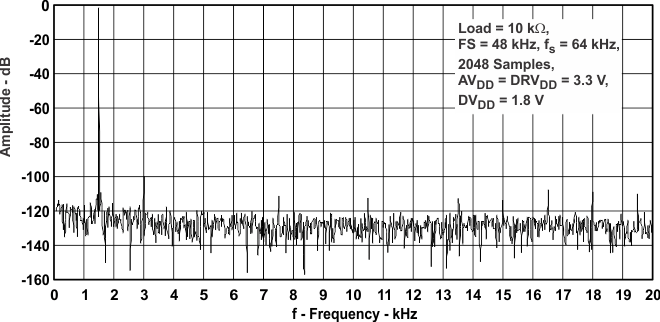
For this design example, use the parameters shown in Table 189.
Table 189. Design Parameters
| PARAMETER | VALUE |
|---|---|
| Supply Voltage (AVDD, DRVDD) | 3.3 V |
| Supply Voltage (DVDD, IOVDD) | 1.8 V |
| Analog Fully Differential Line Output Driver load | 10 kΩ |
10.2.2 Detailed Design Procedure
Using Figure 39 as a guide, integrate the hardware into the system.
Follow the schematic layout and routing in Layout to integrate the device and its supporting components into the system PCB file.
As the TLV320AIC3106-Q1 can be controlled with I2C or SPI protocol, the selection pin of the device must be connected properly.
Determining sample rate and master clock frequency is required when powering up the device because all internal timing is derived from the master clock. See Audio Clock Generation for more information on how to configure correctly the required clocks for the device.
As the TLV320AIC3106-Q1 is designed for low-power applications, when powered up, the device has several features powered down. A correct routing of the TLV320AIC3106-Q1 signals is achieved by a correct setting of the device registers, powering up the required stages of the device and configuring the internal switches to follow a desired route.
10.2.3 Application Curves
 Figure 40. Right DAC FFT
 Figure 42. Signal-To-Noise Ratio vs ADC PGA Setting
 Figure 41. Right ADC FFT