SLAS671C February 2010 – January 2017 TLV320DAC3100
PRODUCTION DATA.
- 1 Device Overview
- 2 Revision History
- 3 Pin Configuration and Functions
-
4 Specifications
- 4.1 Absolute Maximum Ratings
- 4.2 ESD Ratings
- 4.3 Recommended Operating Conditions
- 4.4 Thermal Information
- 4.5 Electrical Characteristics
- 4.6 Power Dissipation Ratings
- 4.7 I2S, LJF, and RJF Timing in Master Mode
- 4.8 I2S, LJF, and RJF Timing in Slave Mode
- 4.9 DSP Timing in Master Mode
- 4.10 DSP Timing in Slave Mode
- 4.11 I2C Interface Timing
- 4.12 Typical Characteristics
- 5 Parameter Measurement Information
-
6 Detailed Description
- 6.1 Overview
- 6.2 Functional Block Diagram
- 6.3
Feature Description
- 6.3.1 Power-Supply Sequence
- 6.3.2 Reset
- 6.3.3 Device Start-Up Lockout Times
- 6.3.4 PLL Start-Up
- 6.3.5 Power-Stage Reset
- 6.3.6 Software Power Down
- 6.3.7 Audio Analog I/O
- 6.3.8
Digital Processing Low-Power Modes
- 6.3.8.1 DAC Playback on Headphones, Stereo, 48 kHz, DVDD = 1.8 V, AVDD = 3.3 V, HPVDD = 3.3 V
- 6.3.8.2 DAC Playback on Headphones, Mono, 48 kHz, DVDD = 1.8 V, AVDD = 3.3 V, HPVDD = 3.3 V
- 6.3.8.3 DAC Playback on Headphones, Stereo, 8 kHz, DVDD = 1.8 V, AVDD = 3.3 V, HPVDD = 3.3 V
- 6.3.8.4 DAC Playback on Headphones, Mono, 8 kHz, DVDD = 1.8 V, AVDD = 3.3 V, HPVDD = 3.3 V
- 6.3.8.5 DAC Playback on Headphones, Stereo, 192 kHz, DVDD = 1.8 V, AVDD = 3.3 V, HPVDD = 3.3 V
- 6.3.8.6 DAC Playback on Line Out (10 k-Ω load), Stereo, 48 kHz, DVDD = 1.8 V, AVDD = 3 V, HPVDD = 3 V
- 6.3.9 Analog Signals
- 6.3.10
Audio DAC and Audio Analog Outputs
- 6.3.10.1
DAC
- 6.3.10.1.1 DAC Processing Blocks
- 6.3.10.1.2
DAC Processing Blocks — Details
- 6.3.10.1.2.1 Three Biquads, Filter A
- 6.3.10.1.2.2 Six Biquads, First-Order IIR, DRC, Filter A or B
- 6.3.10.1.2.3 Six Biquads, First-Order IIR, Filter A or B
- 6.3.10.1.2.4 IIR, Filter B or C
- 6.3.10.1.2.5 Four Biquads, DRC, Filter B
- 6.3.10.1.2.6 Four Biquads, Filter B
- 6.3.10.1.2.7 Four Biquads, First-Order IIR, DRC, Filter C
- 6.3.10.1.2.8 Four Biquads, First-Order IIR, Filter C
- 6.3.10.1.2.9 Two Biquads, 3D, Filter A
- 6.3.10.1.2.10 Five Biquads, DRC, 3D, Filter A
- 6.3.10.1.2.11 Five Biquads, DRC, 3D, Beep Generator, Filter A
- 6.3.10.1.3 DAC User-Programmable Filters
- 6.3.10.1.4 DAC Interpolation Filter Characteristics
- 6.3.10.2 DAC Digital-Volume Control
- 6.3.10.3 Volume Control Pin
- 6.3.10.4 Dynamic Range Compression
- 6.3.10.5 Headphone Detection
- 6.3.10.6 Interrupts
- 6.3.10.7 Key-Click Functionality With Digital Sine-Wave Generator (PRB_P25)
- 6.3.10.8 Programming DAC Digital Filter Coefficients
- 6.3.10.9 Updating DAC Digital Filter Coefficients During PLAY
- 6.3.10.10 Digital Mixing and Routing
- 6.3.10.11 Analog Audio Routing
- 6.3.10.12 Analog Outputs
- 6.3.10.13 Audio-Output Stage-Power Configurations
- 6.3.10.14 DAC Setup
- 6.3.10.15 Example Register Setup to Play Digital Data Through DAC and Headphone/Speaker Outputs
- 6.3.10.1
DAC
- 6.3.11 CLOCK Generation and PLL
- 6.3.12 Timer
- 6.3.13 Digital Audio and Control Interface
- 6.4
Register Map
- 6.4.1 TLV320DAC3100 Register Map
- 6.4.2
Registers
- 6.4.2.1 Control Registers, Page 0 (Default Page): Clock Multipliers, Dividers, Serial Interfaces, Flags, Interrupts, and GPIOs
- 6.4.2.2 Control Registers, Page 1: DAC, Power-Controls, and MISC Logic-Related Programmability
- 6.4.2.3 Control Registers, Page 3: MCLK Divider for Programmable Delay Timer
- 6.4.2.4 Control Registers, Page 8: DAC Programmable Coefficients RAM Buffer A (1:63)
- 6.4.2.5 Control Registers, Page 9: DAC Programmable Coefficients RAM Buffer A (65:127)
- 6.4.2.6 Control Registers, Page 12: DAC Programmable Coefficients RAM Buffer B (1:63)
- 6.4.2.7 Control Registers, Page 13: DAC Programmable Coefficients RAM Buffer B (65:127)
- 7 Application and Implementation
- 8 Power Supply Recommendations
- 9 Layout
- 10Device and Documentation Support
- 11Mechanical Packaging and Orderable Information
Package Options
Mechanical Data (Package|Pins)
- RHB|32
Thermal pad, mechanical data (Package|Pins)
- RHB|32
Orderable Information
7 Application and Implementation
NOTE
Information in the following applications sections is not part of the TI component specification, and TI does not warrant its accuracy or completeness. TI’s customers are responsible for determining suitability of components for their purposes. Customers should validate and test their design implementation to confirm system functionality.
7.1 Application Information
This typical connection highlights the required external components and system level connections for proper operation of the device in several popular use cases.
Each of these configurations can be realized using the Evaluation Modules (EVMs) for the device. These flexible modules allow full evaluation of the device in the most common modes of operation. Any design variation can be supported by TI through schematic and layout reviews. Visit http://e2e.ti.com for design assistance and join the audio amplifier discussion forum for additional information.
7.2 Typical Application
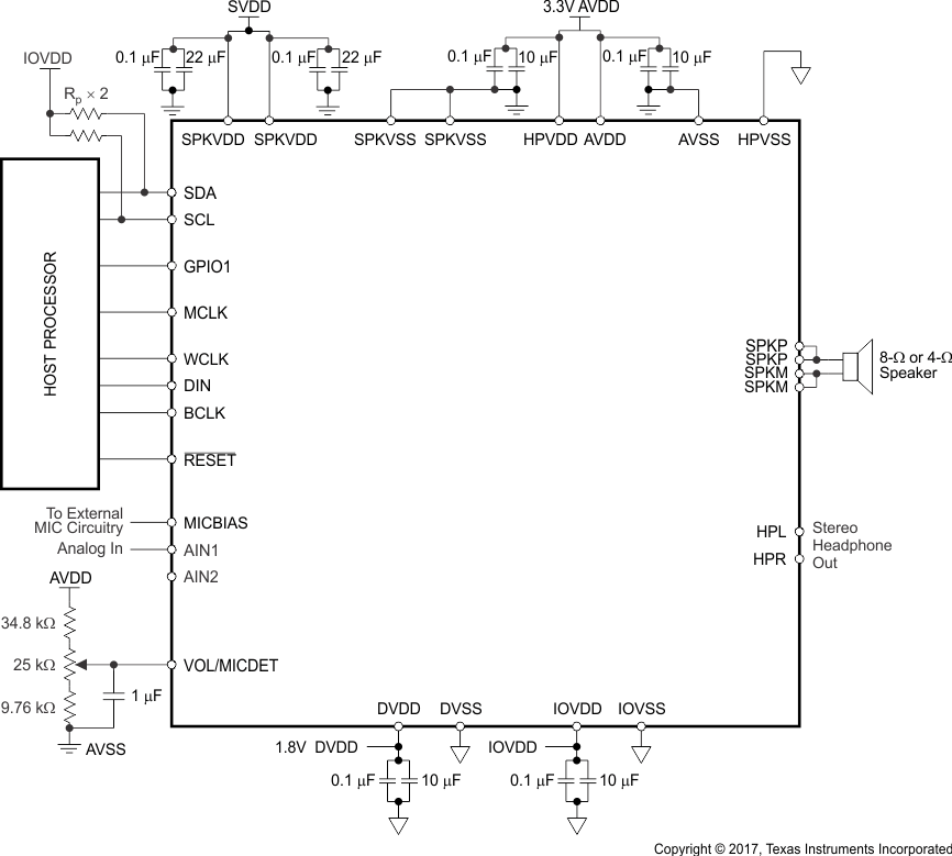
The following application shows the minimal requirements and connections for the TLV320DAC3100 usage. This application shows the usage of a headphone output (HPLOUT, HPROUT) and speaker output (SPKP, SPKM). Additionally, a host processor is used for I2C control and Data Interface.
 Figure 7-1 Typical Circuit Configuration
7.2.1 Design Requirements
For this design example, use the parameters listed in Table 7-1 as the input parameters.
Table 7-1 Design Parameters
| DESIGN PARAMETER | EXAMPLE VALUE |
|---|---|
| AVDD | 3.3 V |
| DVDD | 1.8 V |
| HPVDD | 3.3 V |
| IOVDD | 3.3 A |
| Maximum MICBIAS current | 4 mA |
| SPKVDD | 5 V |
| Power consumption (playback) | 25.62 mW (PRB_P1, 48 kHz, DOSR = 128, stereo headphones) |
7.2.2 Detailed Design Procedure
Using Figure 7-1 as a guide, integrate the hardware into the system.
Following the recommended component placement, schematic layout and routing given in Section 9, integrate the device and its supporting components into the system PCB file. For questions and support, go to the E2E forums (e2e.ti.com). If it is necessary to deviate from the recommended layout, visit the E2E forum to request a layout review.
Determining sample rate and master clock frequency is required since powering up the device as all internal timing is derived from the master clock. Refer to Section 6.3.11 to get more information of how to configure correctly the required clocks for the device.
As the TLV320DAC3100 is designed for low-power applications, when powered up, the device has several features powered down. A correct routing of the TLV320DAC3100 signals is achieved by a correct setting of the device registers, powering up the required stages of the device and configuring the internal switches to follow a desired route. For more information of the device configuration and programming, refer to the TLV320DAC3100's technical documents on ti.com.
7.2.3 Application Curves
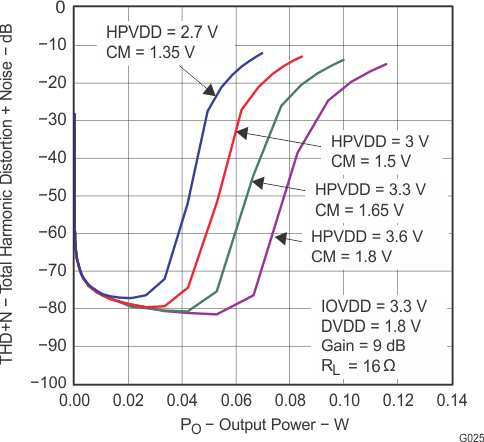
 Figure 7-2 Headphone Output Power
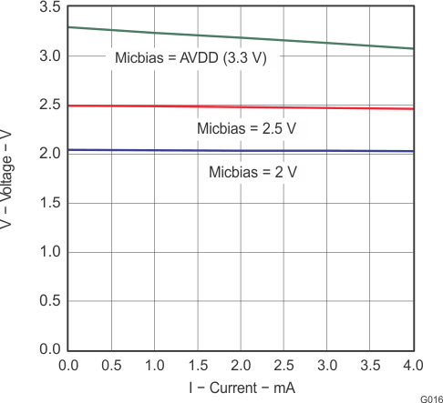
 Figure 7-3 MICBIAS