SNOSDJ0A August   2024  – September 2024 TLV3231

PRODMIX  

  1.   1
  2. Features
  3. Applications
  4. Description
  5. Pin Configuration and Functions
    1.     Pin Configurations: TLV3231 and TLV3232
  6. Specifications
    1. 5.1 Absolute Maximum Ratings
    2. 5.2 ESD Ratings
    3. 5.3 Recommended Operating Conditions
    4. 5.4 Thermal Information
    5. 5.5 Electrical Characteristics
    6. 5.6 Switching Characteristics
    7. 5.7 Typical Characteristics
  7. Detailed Description
    1. 6.1 Overview
    2. 6.2 Functional Block Diagrams
    3. 6.3 Feature Description
    4. 6.4 Device Functional Modes
      1. 6.4.1 Inputs
        1. 6.4.1.1 Unused Inputs
      2. 6.4.2 Internal Hysteresis
      3. 6.4.3 Outputs
      4. 6.4.4 ESD Protection
  8. Application and Implementation
    1. 7.1 Application Information
      1. 7.1.1 Basic Comparator Definitions
        1. 7.1.1.1 Operation
        2. 7.1.1.2 Propagation Delay
        3. 7.1.1.3 Overdrive Voltage
      2. 7.1.2 Hysteresis
        1. 7.1.2.1 Inverting Comparator With Hysteresis
        2. 7.1.2.2 Non-Inverting Comparator With Hysteresis
    2. 7.2 Typical Applications
      1. 7.2.1 Low-Side Current Sensing
        1. 7.2.1.1 Design Requirements
        2. 7.2.1.2 Detailed Design Procedure
        3. 7.2.1.3 Application Curve
    3. 7.3 Power Supply Recommendations
    4. 7.4 Layout
      1. 7.4.1 Layout Guidelines
      2. 7.4.2 Layout Example
  9. Device and Documentation Support
    1. 8.1 Documentation Support
      1. 8.1.1 Related Documentation
    2. 8.2 Receiving Notification of Documentation Updates
    3. 8.3 Support Resources
    4. 8.4 Trademarks
    5. 8.5 Electrostatic Discharge Caution
    6. 8.6 Glossary
  10. Revision History
  11. 10Mechanical, Packaging, and Orderable Information

Package Options

Mechanical Data (Package|Pins)
Thermal pad, mechanical data (Package|Pins)
Orderable Information

Pin Configurations: TLV3231 and TLV3232
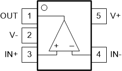
TLV3231 TLV3232 DCK, DBV PackagesSC70,
                            SOT-23-5Top View(Standard "North West"
                            Pinout)DCK, DBV Packages
SC70, SOT-23-5
Top View
(Standard "North West" Pinout)
Table 4-1 Pin Functions: TLV3231
PINI/ODESCRIPTION
NAME

NO.

OUT1OOutput
V-2-Negative supply voltage
IN+3INon-inverting (+) input
IN-4IInverting (-) input
V+5-Positive supply voltage
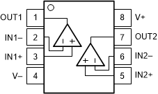
TLV3231 TLV3232 DGK, DSG Packages8-Pin VSSOP, WSONTop View Figure 4-1 DGK, DSG Packages
8-Pin VSSOP, WSON
Top View
Table 4-2 Pin Functions: TLV3232
PIN I/O DESCRIPTION
NAME NO.
IN1+

1

I Noninverting input, channel 1
IN1–

2

I Inverting input, channel 1
IN2–

3

I Inverting input, channel 2
IN2+

4

I Noninverting input, channel 2
OUT1

7

O Output, channel 1
OUT2

6

O Output, channel 2
V-

5

- Negative (lowest) supply or ground
V+ 8 - Positive (highest) supply