SNOSDJ0A August 2024 – September 2024 TLV3231
PRODMIX
- 1
- 1 Features
- 2 Applications
- 3 Description
- 4 Pin Configuration and Functions
- 5 Specifications
- 6 Detailed Description
- 7 Application and Implementation
- 8 Device and Documentation Support
- 9 Revision History
- 10Mechanical, Packaging, and Orderable Information
Package Options
Mechanical Data (Package|Pins)
Thermal pad, mechanical data (Package|Pins)
Orderable Information
3 Description
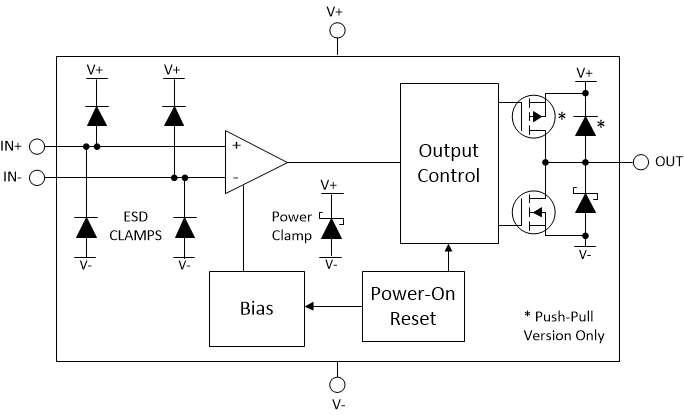
The TLV323x are a family of 5V single and dual channel comparators with push-pull outputs. The family has an excellent speed-to-power combination with a propagation delay of 20ns and a full supply voltage range of 2.7V to 5V with a quiescent supply current of only 200μA per channel.
Likewise, the TLV323x are conveniently available in standard leaded and leadless packages with features such as rail-to-rail inputs, low offset voltage, and large output drive current. These features along with fast response time make the comparators well-suited for current sensing, zero-cross detection, and a variety of other applications where precision and speed is critical.All devices are specified for operation across the expanded temperature range of –40°C to 125°C.
Device Information
| PART NUMBER | PACKAGE (1) | BODY SIZE (NOM (2) |
|---|---|---|
|
TLV3231 |
SC-70 (5) | 1.25mm × 2.00mm |
| SOT-23 (5) | 1.60mm × 2.90mm | |
|
TLV3232 |
VSSOP (8) (Preview) | 3.00mm × 3.00mm |
| WSON (8) (Preview) | 2.00mm × 2.00mm |
(1) For all available packages, see the orderable addendum at the
end of the data sheet.
(2) The package size (length × width) is a nominal value and includes pins,
where applicable.
 Block Diagram
 Low-Side Current Sensing