SBOS533B September 2010 – October 2015 TLV3501A-Q1
PRODUCTION DATA.
- 1 Features
- 2 Applications
- 3 Description
- 4 Revision History
- 5 Related Products
- 6 Pin Configuration and Functions
- 7 Specifications
- 8 Detailed Description
- 9 Application and Implementation
- 10Power Supply Recommendations
- 11Layout
- 12Device and Documentation Support
- 13Mechanical, Packaging, and Orderable Information
Package Options
Mechanical Data (Package|Pins)
- DBV|6
Thermal pad, mechanical data (Package|Pins)
Orderable Information
1 Features
- Qualified for Automotive Applications
- AEC-Q100 Qualified With the Following Results:
- Device Temperature Grade 1: –40°C to +125°C Ambient Operating Temperature Range
- Device HBM Classification Level 2
- Device CDM Classification Level C4B
- High Speed: 4.5 ns
- Rail-To-Rail I/O
- Supply Voltage: 2.7 V to 5.5 V
- Push-Pull CMOS Output Stage
- Shutdown
- Micro Package: SOT23-6
- Low Supply Current: 3.2 mA
- Z-Suffix Offers Improved Delamination
2 Applications
- HEV/EV and Powertrain Applications
- DC-DC Converter
- Inverter
- Fuel Sensing
- Hybrid Power Control Unit
- Automatic Test Equipment
- Threshold Detector
- Zero-Crossing Detector
- Window Comparator
3 Description
The TLV3501A-Q1 push-pull output comparator features a fast 4.5-ns propagation delay and operation from 2.7 V to 5.5 V. The input voltage supports a common-mode range that goes beyond the rails which makes the device an ideal choice for low-voltage applications. The rail-to-rail output directly drives either CMOS or TTL logic. The fast delay and wide common-mode range also makes TLV3501A-Q1 device ideal for EMI reduction through frequency dithering by lowering the EMI peaks. These parameters allow the device to be ideal for both DC-DC converter and inverter applications in HEV/EV and powertrain.
The SOT23-6 microsized package provides options for portable and space-restricted applications. The Z-suffix offers reduced delamination compared to the standard device.
Device Information(1)
| PART NUMBER | PACKAGE | BODY SIZE (NOM) |
|---|---|---|
| TLV3501A-Q1 | SOT-23 (6) | 2.90 mm × 1.60 mm |
- For all available packages, see the orderable addendum at the end of the datasheet.
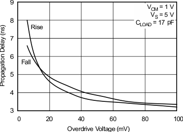
Propagation Delay vs Overdrive Voltage
