SBOS533B September 2010 – October 2015 TLV3501A-Q1
PRODUCTION DATA.
- 1 Features
- 2 Applications
- 3 Description
- 4 Revision History
- 5 Related Products
- 6 Pin Configuration and Functions
- 7 Specifications
- 8 Detailed Description
- 9 Application and Implementation
- 10Power Supply Recommendations
- 11Layout
- 12Device and Documentation Support
- 13Mechanical, Packaging, and Orderable Information
Package Options
Mechanical Data (Package|Pins)
- DBV|6
Thermal pad, mechanical data (Package|Pins)
Orderable Information
8 Detailed Description
8.1 Overview
The TLV3501A-Q1 device features high-speed response and includes 6 mV of internal hysteresis for improved noise immunity with an input common-mode range that extends 0.2 V beyond the power-supply rails.
8.2 Functional Block Diagram

8.3 Feature Description
8.3.1 Operating Voltage
The TLV3501A-Q1 comparators are specified for use on a single supply from 2.7 V to 5.5 V (or a dual supply from ±1.35 V to ±2.75 V) over a temperature range of −40°C to +125°C. The device continues to function below this range, but performance is not specified.
8.3.2 Input Overvoltage Protection
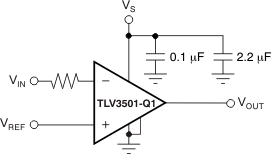
The device inputs are protected by electrostatic discharge (ESD) diodes that conduct if the input voltages exceed the power supplies by more than approximately 300 mV. Momentary voltages greater than 300 mV beyond the power supply can be tolerated if the input current is limited to 10 mA. This limiting is easily accomplished with a small input resistor in series with the comparator, as shown in Figure 15.
 Figure 15. Input Current Protection for Voltages Exceeding the Supply Voltage
8.4 Device Functional Modes
8.4.1 Shutdown
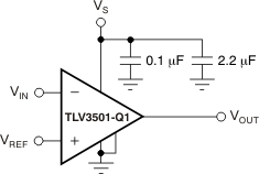
A shutdown pin (SHDN) allows the device to go idle when the SHDN pin is not in use. When the SHDN pin is high, the device draws about 2 μA and the output goes to high impedance. When the shutdown pin is low, the TLV3501A-Q1 device is active. When the TLV3501A-Q1 shutdown feature is not used, connect the shutdown pin to the most negative supply, as shown in Figure 16. Exiting shutdown mode takes about 100 ns.
 Figure 16. Basic Connections for the TLV3501A-Q1