SBOS507A February 2010 – December 2014 TLV3502-Q1
PRODUCTION DATA.
- 1 Features
- 2 Applications
- 3 Description
- 4 Revision History
- 5 Pin Configuration and Functions
- 6 Specifications
- 7 Detailed Description
- 8 Application and Implementation
- 9 Power Supply Recommendations
- 10Layout
- 11Device and Documentation Support
- 12Mechanical, Packaging, and Orderable Information
Package Options
Mechanical Data (Package|Pins)
- DCN|8
Thermal pad, mechanical data (Package|Pins)
- DCN|8
Orderable Information
7 Detailed Description
7.1 Overview
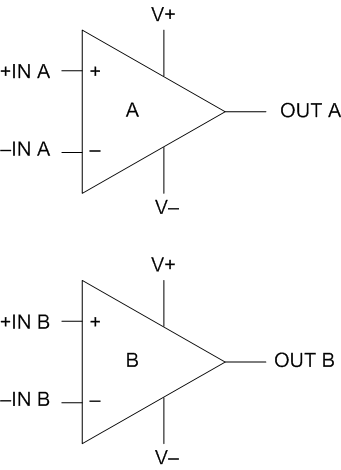
The TLV3502-Q1 push-pull output comparator features a fast 4.5-ns propagation delay and operation from 2.7 V to 5.5 V. Beyond-the-rails input common-mode range makes it an ideal choice for low-voltage applications. The rail-to-rail output directly drives either CMOS or TTL logic.
7.2 Functional Block Diagram
7.3 Feature Description
The TLV3502-Q1 device feature fast 4.5-ns propagation delay with a push-pull output. The device operates from 2.7 V to 5.5 V. It has beyond-the-rails input common-mode range and rail-to-rail output directly drives either CMOS or TTL logic.
7.3.1 Input Over-Voltage Protection
Device inputs are protected by ESD diodes that will conduct if the input voltages exceed the power supplies by more than approximately 300 mV. Momentary voltages greater than 300 mV beyond the power supply can be tolerated if the input current is limited to 10 mA. This limiting is easily accomplished with a small input resistor in series with the comparator, as shown in Figure 15.
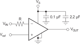 Figure 15. Input Current Protection for Voltages Exceeding the Supply Voltage
7.3.2 Relaxation Oscillator
The TLV350x can easily be configured as a simple and inexpensive relaxation oscillator. In Figure 16, the R2 network sets the trip threshold at 1/3 and 2/3 of the supply. Since this is a high-speed circuit, the resistor values are rather low to minimize the effect of parasitic capacitance. The positive input alternates between 1/3 of V+ and 2/3 of V+ depending on whether the output is low or high. The time to charge (or discharge) is 0.69R1C. Therefore, the period is 1.38R1C. For 62 pF and 1 kΩ as shown in Figure 16, the output is calculated to be 10.9MHz. An implementation of this circuit oscillated at 9.6 MHz. Parasitic capacitance and component tolerances explain the difference between theory and actual performance.
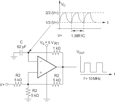 Figure 16. Relaxation Oscillator
7.3.3 High-Speed Window Comparator
A window comparator circuit is used to determine when a signal is between two voltages. The TLV3502-Q1 device can readily be used to create a high-speed window comparator. VHI is the upper voltage threshold, and VLO is the lower voltage threshold. When VIN is between these two thresholds, the output in Figure 17 is high. Figure 18 shows a simple means of obtaining an active low output. Note that the reference levels are connected differently between Figure 17 and Figure 18. The operating voltage range of either circuit is 2.7 V to 5.5 V.
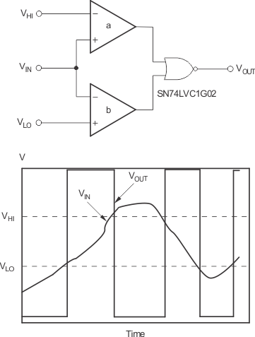 Figure 17. Window Comparator—Active High
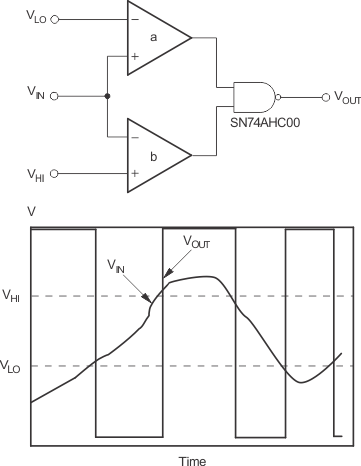 Figure 18. Window Comparator—Active Low
7.4 Device Functional Modes
This device has no special operating modes outside of the normally powered dual comparator function.