SBOS507A February 2010 – December 2014 TLV3502-Q1
PRODUCTION DATA.
- 1 Features
- 2 Applications
- 3 Description
- 4 Revision History
- 5 Pin Configuration and Functions
- 6 Specifications
- 7 Detailed Description
- 8 Application and Implementation
- 9 Power Supply Recommendations
- 10Layout
- 11Device and Documentation Support
- 12Mechanical, Packaging, and Orderable Information
Package Options
Mechanical Data (Package|Pins)
- DCN|8
Thermal pad, mechanical data (Package|Pins)
- DCN|8
Orderable Information
5 Pin Configuration and Functions
8-Pin SOT-23
DCN Package
(Top View)
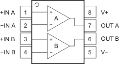
Pin Functions
| PIN | TYPE | DESCRIPTION | |
|---|---|---|---|
| NO. | NAME | ||
| 1 | +IN A | I | Non inverting input, channel A |
| 2 | –IN A | I | Inverting input, channel A |
| 3 | +IN B | I | Non inverting input, channel B |
| 4 | –IN B | I | Inverting input, channel B |
| 5 | V– | Supply | Negative (lowest) power supply |
| 6 | OUT B | O | Output, channel B |
| 7 | OUT A | O | Output, channel A |
| 8 | V+ | Supply | Positive (highest) power supply |