SNOSDL8 November 2024 TLV3511-Q1
ADVANCE INFORMATION
- 1
- 1 Features
- 2 Applications
- 3 Description
- 4 Pin Configuration and Functions
- 5 Specifications
- 6 Detailed Description
- 7 Application and Implementation
- 8 Device and Documentation Support
- 9 Revision History
- 10Mechanical, Packaging, and Orderable Information
Package Options
Mechanical Data (Package|Pins)
- DCK|5
Thermal pad, mechanical data (Package|Pins)
Orderable Information
7.1.2.1 Inverting Comparator With Hysteresis
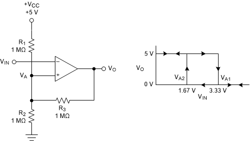
The inverting comparator with hysteresis requires a three-resistor network that is referenced to the comparator supply voltage (VCC), as shown below.
 Figure 7-3 TLV351x-Q1 in an Inverting Configuration With Hysteresis
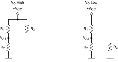
The equivalent resistor networks when the output is high and low are shown below.
 Figure 7-4 Inverting Configuration Resistor Equivalent Networks
When VIN is less than VA, the output voltage is high (for simplicity, assume VO switches as high as VCC). The three network resistors can be represented as R1 || R3 in series with R2, as shown above on the left.
The equation below defines the high-to-low trip voltage (VA1).

When VIN is greater than VA, the output voltage is low. In this case, the three network resistors can be presented as R2 || R3 in series with R1, as shown above on the right.
Use equation below to define the low to high trip voltage (VA2).

The equation below defines the total hysteresis provided by the network.
