SBOS756 October 2016 TLV3541 , TLV3542 , TLV3544
PRODUCTION DATA.
- 1 Features
- 2 Applications
- 3 Description
- 4 Revision History
- 5 Pin Configuration and Functions
- 6 Specifications
- 7 Detailed Description
- 8 Application and Implementation
- 9 Power Supply Recommendations
- 10Layout
- 11Device and Documentation Support
- 12Mechanical, Packaging, and Orderable Information
Package Options
Mechanical Data (Package|Pins)
Thermal pad, mechanical data (Package|Pins)
Orderable Information
8 Application and Implementation
NOTE
Information in the following applications sections is not part of the TI component specification, and TI does not warrant its accuracy or completeness. TI’s customers are responsible for determining suitability of components for their purposes. Customers should validate and test their design implementation to confirm system functionality.
8.1 Application Information
The TLV354x are wide bandwidth, low-noise, rail-to-rail input and output amplifiers. These devices operate from 2.5 V to 5.5 V, are unity-gain stable, and suitable for a wide range of general-purpose applications The input common-mode voltage range includes both rails, and allows the TLV354x device to be used in any single-supply application. Rail-to-rail input and output swing significantly increases dynamic range, especially in low-supply applications, and makes the device ideal for driving analog-to-digital converters (ADCs).
The TLV354x family of devices features a 200-MHz bandwidth and 150-V/μs slew rate with only 7.5 nV/√Hz of broadband noise.
8.2 Typical Application
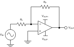
A typical application for an operational amplifier is an inverting amplifier, as shown in Figure 28. An inverting amplifier takes a positive voltage on the input and outputs a signal inverted to the input, making a negative voltage of the same magnitude. In the same manner, the amplifier makes negative input voltages positive on the output. In addition, amplification can be added by selecting the input resistor RI and the feedback resistor RF.
 Figure 28. Application Schematic
8.2.1 Design Requirements
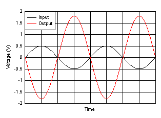
The supply voltage must be chosen to be larger than the input voltage range and the desired output range. The limits of the input common-mode range (VCM) and the output voltage swing to the rails (VO) must be considered. For instance, this application scales a signal of ±0.5 V (1 V) to ±1.8 V (3.6 V). Setting the supply at ±2.5 V is sufficient to accommodate this application.
8.2.2 Detailed Design Procedure
Determine the gain required by the inverting amplifier using Equation 3 and Equation 4:


When the desired gain is determined, select a value for RI or RF. Selecting a value in the kilo ohm range is desirable for general-purpose applications because the amplifier circuit uses currents in the milliamp range. This milliamp current range ensures the device does not draw too much current. The trade-off is that large resistors (100s of kilo ohms) draw the smallest current but generate the highest noise. Small resistors (100s of ohms) generate low noise but draw high current. This example uses 10 kΩ for RI, meaning 36 kΩ is used for RF. These values are determined by Equation 5:

8.2.3 Application Curve
 Figure 29. Inverting Amplifier Input and Output
8.3 System Examples
When receiving low-level signals, limiting the bandwidth of the incoming signals into the system is often required. The simplest way to establish this limited bandwidth is to place an RC filter at the noninverting terminal of the amplifier, as shown in Figure 30.
 Figure 30. Single-Pole, Low-Pass Filter
If even more attenuation is needed, a multiple pole filter is required. The Sallen-Key filter can be used for this task, as shown in Figure 31. For best results, the amplifier must have a bandwidth that is eight to ten times the filter frequency bandwidth. Failure to follow this guideline can result in phase shift of the amplifier.
 Figure 31. Two-Pole, Low-Pass, Sallen-Key Filter